Laser crystallization process and laser process

a laser crystallization and laser technology, applied in the direction of semiconductor/solid-state device manufacturing, basic electric elements, electric devices, etc., can solve the problems of poor crystallization uniformity, easy damage to the device of the lower layer, rough active layer surface, etc., to achieve the effect of bad crystallization uniformity and easy damag

Inactive Publication Date: 2009-02-12
IND TECH RES INST
View PDF6 Cites 0 Cited by
  • Summary
  • Abstract
  • Description
  • Claims
  • Application Information

AI Technical Summary

Benefits of technology

[0008]The present invention further provides a laser process applicable to a fabrication of a flexible display panel. The process solves the problem that the substrate of the flexible display panel would become poor when a laser process is used to perform a conventional crystallization process or a conventional activation process.
[0010]In the present invention, since the multi-layer reflective layer is formed underneath the amorphous silicon islands, the multi-layer reflective layer can reflect a laser light so as to prevent the active devices on the substrate from being damaged. Moreover, the present invention performs the laser annealing step on the amorphous silicon islands so that the amorphous silicon islands are laterally crystallized. Therefore, the active layer formed by such manner has better uniformity and less surface roughness.
[0012]In the present invention, since the multi-layer reflective layer is formed above the substrate, the multi-layer reflective layer can reflect the laser light so as to prevent the substrate from becoming poor for being irradiated by the laser light.

Problems solved by technology

Such defects includes the device of the lower layer being damaged easily, having bad crystallization uniformity and having a rough active layer surface.
The process solves the problem that the substrate of the flexible display panel would become poor when a laser process is used to perform a conventional crystallization process or a conventional activation process.

Method used


Image

  • Laser crystallization process and laser process
  • Laser crystallization process and laser process
  • Laser crystallization process and laser process

Examples


first embodiment

The First Embodiment

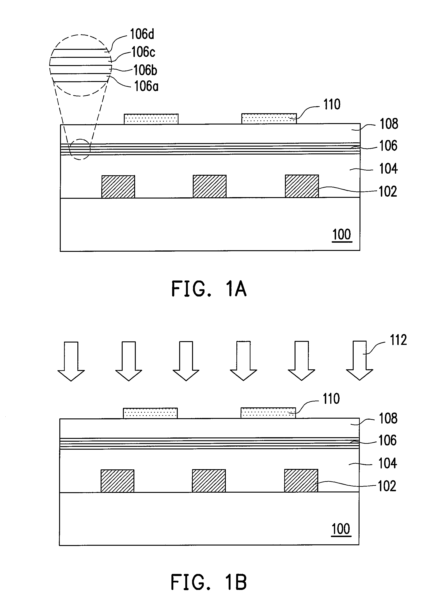
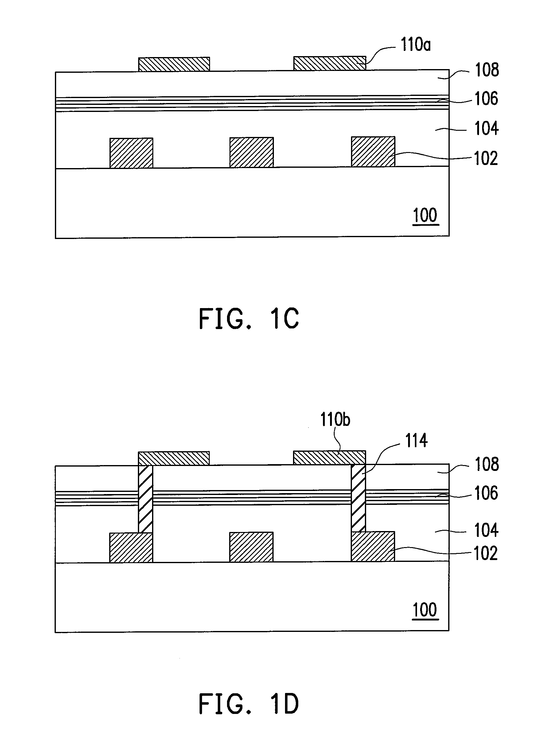
[0016]FIGS. 1A through 1D are schematic views illustrating the laser crystallization process used for forming stack devices according to one embodiment of the present invention. Referring to FIG. 1A, a substrate 100 is provided, which has a plurality of active devices 102 already formed thereon. The substrate 100 may be a wafer or a chip. The active devices 102 are metal-oxide-semiconductor (MOS) transistors, for example. A method for forming the active devices 102 on the substrate 100 adopts a semiconductor fabrication process as known in the prior art, for example. Next, a first dielectric layer 104 is formed above the substrate 100 covering the active devices 102. A material of the first dielectric layer 104 is silicon oxide, silicon nitride, for example. A method for forming the first dielectric layer 104 is a chemical vapor deposition (CVD) process or a coating process.

[0017]Then, a multi-layer reflective layer 106 is formed on the first dielectric layer 104...

second embodiment

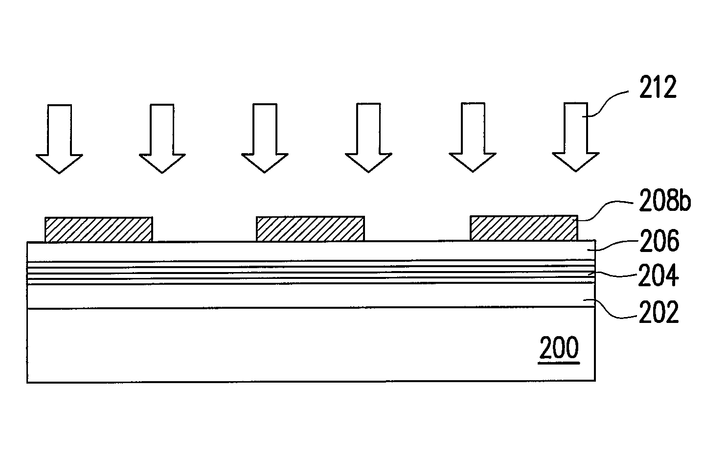
[0026]FIGS. 2A through 2D are schematic views illustrating a laser process used for fabricating a flexible display panel according to one embodiment of the present invention. Referring to FIG. 2A first, a substrate 200 is provided. A material of the substrate 200 includes an organic polymer material, such as polyimide. Generally, the substrate used for a flexible display panel is consisted of the organic polymer material, and therefore, the substrate is flexible.

[0027]Next, a multi-layer reflective layer 204 is formed above the substrate 200. In one embodiment, before forming the multi-layer reflective layer 204, it further includes forming a buffer layer 202 on the substrate 200. The multi-layer reflective layer 204 is formed by alternately stacking at least one high-refractive dielectric material and at least one low-refractive dielectric material. As shown in a magnified view on the left of FIG. 2A, the multi-layer reflective layer 204 is formed by alternately stacking a low-refr...


PUM

PropertyMeasurementUnit
temperatureaaaaaaaaaa
wavelengthaaaaaaaaaa
reflectivityaaaaaaaaaa

Abstract

The present invention provides a laser crystallization process applicable to a fabrication of a stack device structure. The process starts with providing a substrate having active devices formed thereon. Next, a first dielectric layer is formed on the substrate, and a multi-layer reflective layer is formed on the first dielectric layer. Then, a second dielectric layer is formed on the multi-layer reflective layer, and amorphous silicon islands are formed on the second dielectric layer. After that, a laser annealing step is performed so that the amorphous silicon islands are crystallized so as to form a poly-silicon active layer.

Description

CROSS-REFERENCE TO RELATED APPLICATION[0001]This application claims the priority benefit of Taiwan application serial no. 96129381, filed on Aug. 9, 2007. The entirety of the above-mentioned patent application is hereby incorporated by reference herein and made a part of this specification.BACKGROUND OF THE INVENTION[0002]1. Field of the Invention[0003]The present invention is related to a laser crystallization process and a laser process and more particularly to a laser crystallization process applicable to a fabrication of a stack device and a laser process applicable to a flexible display panel.[0004]2. Description of Related Art[0005]With development of the integrated circuit, the requirement for device density becomes gradually higher, and the device size also becomes gradually smaller. In response to such trend, besides enhancing the device density by reducing the device size, satisfying the height of various types of current integrated circuits by stacking is also a good meth...

Claims


Application Information

Patent Timeline
Patent Type & Authority Applications(United States)
IPC IPC(8): H01L21/20
CPCH01L21/02532H01L21/02675H01L21/02658
Inventor CHEN, HUNG-TSE
Owner IND TECH RES INST
Why Eureka
Try Eureka