Method for fabricating semiconductor device and semiconductor device

a semiconductor device and a technology for semiconductors, applied in semiconductor/solid-state device manufacturing, basic electric elements, electric devices, etc., can solve the disadvantageous reduction of reliability of copper ion diffusion preventing films, and achieve the suppression of the lowering of the reliability of a semiconductor device, the reduction of the dielectric constant, and the prevention of copper ions from a copper interconnect

Inactive Publication Date: 2009-02-12
PANASONIC CORP
View PDF9 Cites 2 Cited by
  • Summary
  • Abstract
  • Description
  • Claims
  • Application Information

AI Technical Summary

Benefits of technology

[0010]As a method for overcoming the above-described conventional problem, the following methods have been proposed: An interlayer insulating film that has a low dielectric constant (of 2.5), is thermally stable and has a function to prevent diffusion of copper ions is formed by an inexpensive method in which the working efficiency of a fabrication system is not lowered by using a disiloxane derivative having a simple chemical structure and having a substituent with two or more functional groups and with no thermal polymerization property; and an interlayer insulating film that is good at mechanical strength and has a function to prevent diffusion of copper ions is formed through three-dimensional polymerization using a disiloxane derivative having three or more functional groups.
[0011]In the interlayer insulating film having the copper ion diffusion preventing function formed by the plasma CVD using the disiloxane derivative having a simple chemical structure and having a substituent with two or more functional groups and with no thermal polymerization property, a siloxane site surrounded with organic sites functions as a site for trapping a copper ion. Accordingly, a structure in which a siloxane site is three-dimensionally surrounded with organic sites is the essential condition for providing the copper ion diffusion preventing function.

Problems solved by technology

At the early stage of forming the interlayer insulating film by the plasma CVD, however, the structure in which the siloxane site working as the site for trapping a copper ion is three-dimensionally surrounded with organic sites is not completed yet, and hence, copper ions are easily diffused from a copper interconnect formed below the interlayer insulating film by the heat applied in the deposition process.
Accordingly, even in the interlayer insulating film having the copper ion diffusion preventing function, the diffusion of copper ions cannot be sufficiently prevented at the early stage of the deposition, and hence, the reliability as the copper ion diffusion preventing film is disadvantageously lowered.

Method used


Image

  • Method for fabricating semiconductor device and semiconductor device
  • Method for fabricating semiconductor device and semiconductor device
  • Method for fabricating semiconductor device and semiconductor device

Examples


embodiment 1

[0034]A method for fabricating a semiconductor device according to Embodiment 1 of the invention will now be described with reference to the accompanying drawings.

[0035]FIGS. 1A through 1C are cross-sectional views for showing procedures in the method for fabricating a semiconductor device of Embodiment 1.

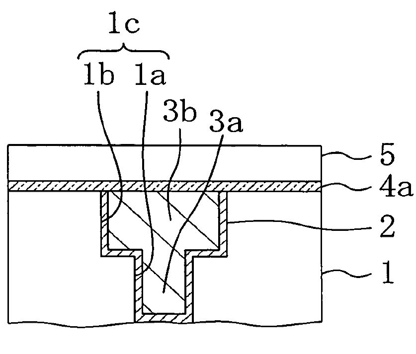
[0036]First, as shown in FIG. 1A, a recess le corresponding to a dual damascene interconnect groove composed of a via hole 1a and an interconnect groove 1b communicated with the via hole 1a is formed in a first interlayer insulating film 1 formed on a semiconductor substrate not shown and made of a low dielectric constant material (a low-k material). Thereafter, a barrier film 2 is formed on the inner wall and the bottom of the recess 1c, so as to prevent the first interlayer insulating film 1 from being in direct contact with an interconnect plug 3a and a copper interconnect 3b described below. Then, copper is filled in the recess 1c where the barrier film 2 has been formed and an...

embodiment 2

[0046]A method for fabricating a semiconductor device according to Embodiment 2 of the invention will now be described with reference to the accompanying drawings.

[0047]FIGS. 3A through 3C are cross-sectional views for showing procedures in the method for fabricating a semiconductor device of Embodiment 2.

[0048]First, as shown in FIG. 3A, a recess 1c corresponding to a dual damascene interconnect groove composed of a via hole 1a and an interconnect groove 1b communicated with the via hole 1a is formed in a first interlayer insulating film 1 formed on a semiconductor substrate not shown and made of a low dielectric constant material (a low-k material). Thereafter, a barrier film 2 is formed on the inner wall and the bottom of the recess 1c so as to prevent the first interlayer insulating film 1 from being in direct contact with an interconnect plug 3a and a copper interconnect 3b described below. Then, copper is filled within the recess 1c where the barrier film 2 has been formed and...

embodiment 3

[0053]A method for fabricating a semiconductor device according to Embodiment 3 of the invention will now be described with reference to the accompanying drawings.

[0054]FIGS. 4A through 4C are cross-sectional views for showing procedures in the method for fabricating a semiconductor device of Embodiment 3.

[0055]First, as shown in FIG. 4A, a recess 1c corresponding to a dual damascene interconnect groove composed of a via hole 1a and an interconnect groove 1b communicated with the via hole 1a is formed in a first interlayer insulating film 1 formed on a semiconductor substrate not shown and made of a low dielectric constant material (a low-k material). Thereafter, a barrier film 2 is formed on the inner wall and the bottom of the recess 1c, so as to prevent the first interlayer insulating film 1 from being in direct contact with an interconnect plug 3a and a copper interconnect 3b described below. Then, copper is filled within the recess 1c where the barrier film 2 has been formed an...


PUM

PropertyMeasurementUnit
dielectric constantaaaaaaaaaa
temperatureaaaaaaaaaa

Abstract

A method for fabricating a semiconductor device includes the steps of forming a nitrogen-containing layer in an exposed portion of a copper interconnect formed in an insulating film provided on a substrate; and forming an interlayer insulating film on the nitrogen-containing layer through plasma CVD performed by using, as a material, an organic silicon compound having a siloxane (Si—O—Si) bond.

Description

CROSS-REFERENCE TO RELATED APPLICATIONS[0001]This application claims priority under 35 U.S.C. §119 on Patent Application No. 2005-180604 filed in Japan on June 21, 2005, the entire contents of which are hereby incorporated by reference.BACKGROUND OF THE INVENTION[0002]The present invention relates to a method for fabricating a semiconductor device and the semiconductor device fabricated by the method, and more particularly, it relates to a method for fabricating a semiconductor device including a low dielectric constant insulating film having a function to prevent diffusion of copper ions and the semiconductor device fabricated by the method.[0003]As an insulating film to be used as a copper diffusion preventing film in very large scale integration (VLSI) having copper interconnects, a SiN film, a SiON film, a SiC film, a SiCO film or the like is conventionally known, and all of these insulating films have a high dielectric constant of 4 or more. Therefore, even when a low dielectri...

Claims


Application Information

Patent Timeline
Patent Type & Authority Applications(United States)
IPC IPC(8): H01L21/31
CPCH01L21/02126H01L21/02216H01L21/02274H01L21/02304H01L21/31633H01L21/76886H01L21/76832H01L21/76834H01L21/76849H01L21/76867H01L21/3185
Inventor AOI, NOBUONAKAGAWA, HIDEO
Owner PANASONIC CORP
Why Eureka
Try Eureka