Semiconductor device, epitaxial wafer, and method of manufacturing the same

a semiconductor device and epitaxial wafer technology, applied in the field of semiconductor devices and epitaxial wafers, can solve the problems of failure of semiconductor devices including these p elements, affecting the quality of semiconductor devices, and reducing the concentration of semiconductor devices, so as to improve the crystal quality reduce the average hydrogen concentration of the n-containing ingaas-based layer, and improve the quality of the stacked structure of high-quality

Inactive Publication Date: 2009-03-05
SUMITOMO ELECTRIC IND LTD
View PDF0 Cites 29 Cited by
  • Summary
  • Abstract
  • Description
  • Claims
  • Application Information

AI Technical Summary

Benefits of technology

[0009]According to the above-mentioned method, since the N-containing InGaAs-based layer is formed by the MBE method in which a raw material that does not contain hydrogen (H) in the chemical formula thereof is used, the hydrogen is limited to the thickness range at an early stage of forming the N-containing InGaAa-based layer, and accordingly a high-concentration hydrogen layer is formed only in a narrow thickness range limited from the bottom face of the N-containing InGaAa-based layer. Hereinafter, the MBE method is assumed to use a raw material that does not contain H in the chemical formula. In the upper side above the high-concentration hydrogen layer, the hydrogen concentration can be suppressed to be lower. Therefore, by a heat treatment of such a low temperature as in the range of 600° C. or more to less than 800° C., the hydrogen can be reduced to a low level that will not cause a significant problem. As a result, both the hydrogen peak value of the high-concentration hydrogen layer and the hydrogen concentration of substantially flat distribution in a layer upper than the high-concentration hydrogen layer can be decreased by the heat treatment, and accordingly the average hydrogen concentration of the N-containing InGaAs-based layer can be decreased. Therefore, the crystal quality of the N-containing InGaAs-based layer can be enhanced, and consequently a high quality semiconductor stacked structure or semiconductor device can easily be manufactured. Here, the ground of the N-containing InGaAs-based layer corresponds to a buffer layer that is epitaxially formed in contact with an InP substrate; however, it may be a ground other than the buffer layer, that is, it may be an InP substrate, for example.

Problems solved by technology

The hydrogen concentration must be reduced because, if hydrogen mixes with GaInNAs, defects that play a role of donors are formed, whereby the density of lattice defects is increased, resulting in degradation of the crystal quality.
However, if P-containing compound semiconductors, such as an InP substrate and the like, are heated at such a high temperature as mentioned above, dephosphorization phenomenon occurs, resulting in malfunction of the semiconductor devices including these P elements.
In addition to such dephosphorization, other problems will occur, making it difficult to form semiconductor devices such as a photodiode.

Method used


Image

  • Semiconductor device, epitaxial wafer, and method of manufacturing the same
  • Semiconductor device, epitaxial wafer, and method of manufacturing the same
  • Semiconductor device, epitaxial wafer, and method of manufacturing the same

Examples


embodiment 1

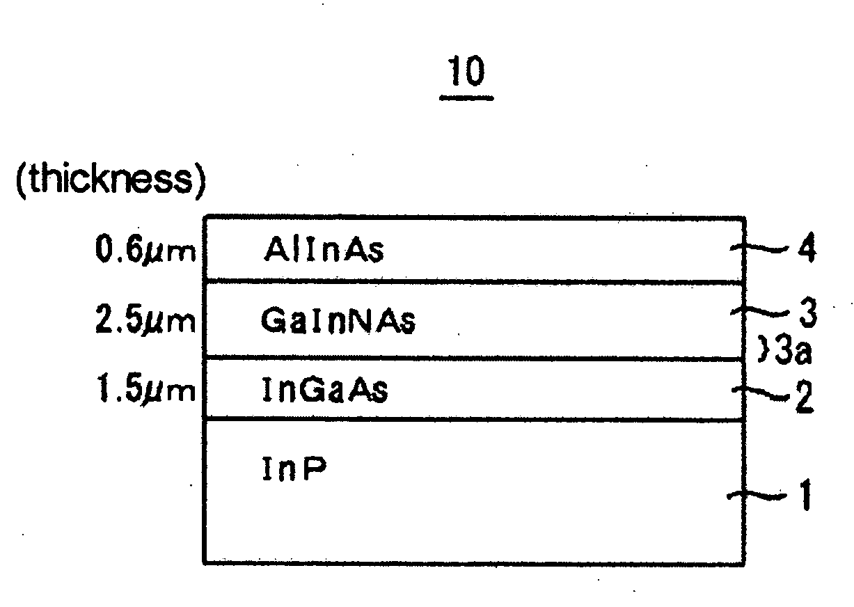
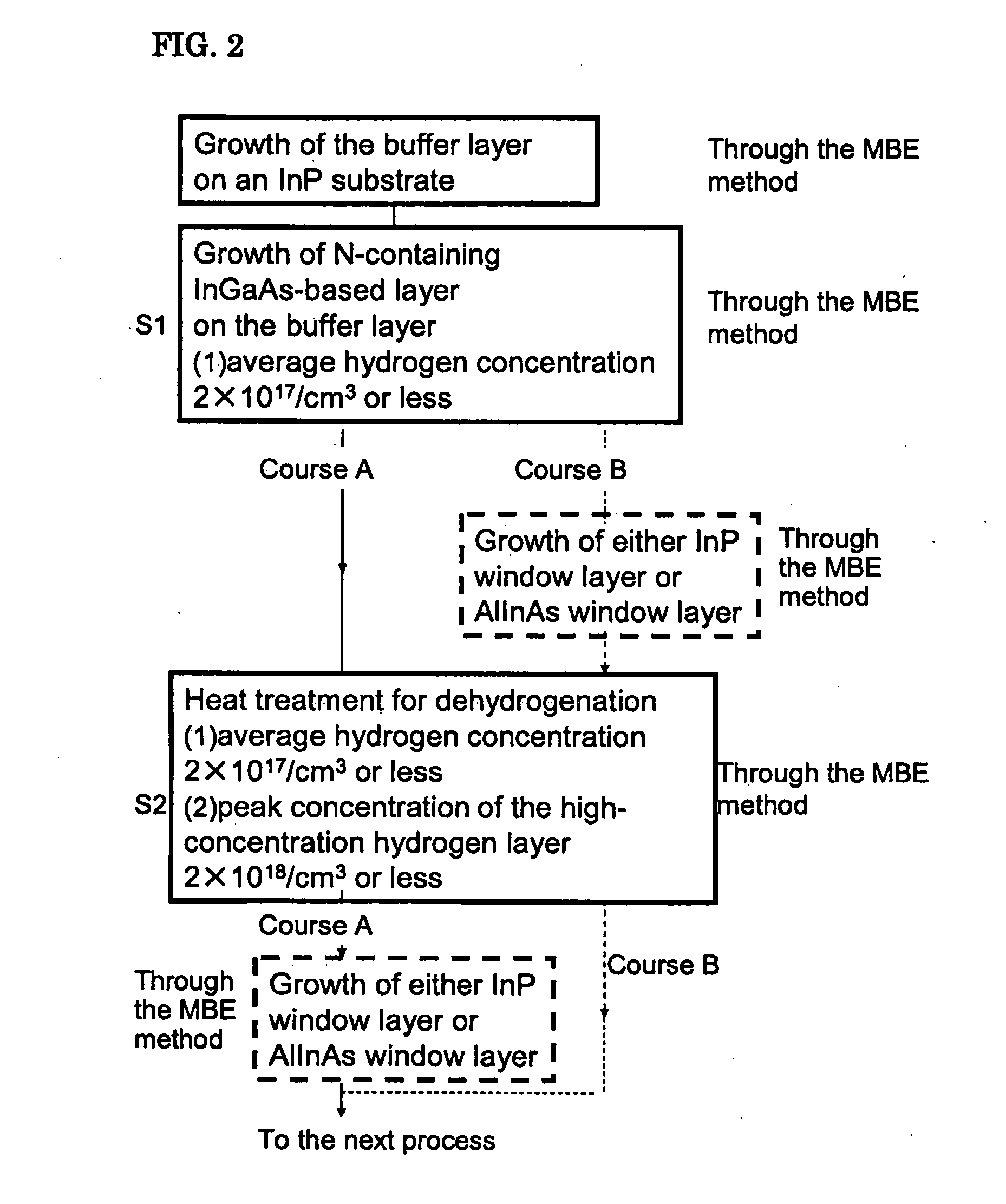
[0031]FIG. 1 is a sectional view showing a stacked structure 10 of a semiconductor device in Embodiment 1 of the present invention. The stacked structure 10 is formed of compound semiconductor layers as described in the following. The epitaxial wafer, which is regarded as an intermediate product for forming a semiconductor device including the stacked structure 10, is sold as such on the market. Hereinafter, the term “semiconductor device” used in the description of a compound semiconductor layer includes an epitaxial wafer. Stacked structure 10: (InP substrate 1 / InGaAs buffer layer 2 / GaInNAs receiving layer 3 / AlInAs window layer 4)

[0032]The thickness of each layer is roughly as follows: InGaAs buffer layer 2 is about 1 μm to 2 μm; GaInNAs light-receiving layer 3, which is an N-containing InGaAs-based layer, is 2 μm to 3 μm; and AlInAs window layer 4 is 0.5 μm to 1.5 μm. In the case where a semiconductor photodetector is a photodiode, a mask pattern is provided on the AlInAs window ...


PUM

PropertyMeasurementUnit
temperatureaaaaaaaaaa
thicknessaaaaaaaaaa

Abstract

A manufacturing method and a semiconductor device produced by the method are provided, in which the semiconductor device can easily be manufactured while the hydrogen concentration is decreased. An N-containing InGaAs layer 3 is grown on an InP substrate by the MBE method, and thereafter a heat treatment is provided at a temperature in the range of 600° C. or more and less than 800° C., whereby the average hydrogen concentration of the N-containing InGaAs layer 3 is made equal to or 2×10¹⁷/cm3 or less than.

Description

BACKGROUND OF THE INVENTION[0001]1. Field of the Invention[0002]The present invention relates to a semiconductor device, an epitaxial wafer, and the method of manufacturing the same. More specifically, the invention relates to a semiconductor device or an epitaxial wafer which has an N-containing InGaAs-based layer, and a method of manufacturing the same.[0003]2. Description of the Background Art[0004]It is known that the degradation of crystal quality is caused by mixing of high concentration of hydrogen into GaNAs and GaInNAs including In-composition of 35% or less in III-group elements that have been grown on a Gabs substrate by the OMVPE method. Therefore, in the method proposed in Japanese Patent Application Publication No. H11-274083 (Patent document 1), the hydrogen concentration is reduced by performing heat treatment for dehydrogenation after growing the above-mentioned semiconductor layer on a GaAs substrate by the OMVPE method. According to this method, it is possible to ...

Claims


Application Information

Patent Timeline
Patent Type & Authority Applications(United States)
IPC IPC(8): H01L21/20H01L29/20
CPCH01L21/02392H01L21/02463H01L21/0254H01L21/02543H01L21/02546Y02E10/544H01L21/02631H01L21/02664H01L31/109H01L31/1844H01L21/02549Y02P70/50
Inventor MIURA, KOUHEIIGUCHI, YASUHIRO
Owner SUMITOMO ELECTRIC IND LTD
Why Eureka
Try Eureka