Semiconductor memory device having vertical transistors

Active Publication Date: 2009-03-05
LONGITUDE LICENSING LTD
View PDF5 Cites 60 Cited by
  • Summary
  • Abstract
  • Description
  • Claims
  • Application Information

AI Technical Summary

Benefits of technology

[0016]According to the aspects of the invention, in the memory cell array region, the plurality of memory cells each formed using the vertical transistor is arranged at intersections of the word lines and the bit lines. Meanwhile, the vertical transistors in the end region in which no word line is provided are connected to the predetermined circuit arranged overlapping the memory cell array region and the peripheral circuit region. When the predetermined circuit is formed only in the peripheral circuit region, the transistor size increases and the arrangement becomes irregular, and therefore an increase in the area is inevitable. On the other hand, the present invention enables that part of the predetermined circuit is formed by utilizing the vertical transistors which can be arranged in a small size and with high density in the same manner as the memory cell array. Thus, the occupied area of the predetermined circuit can be reliably reduced, and a semiconductor memory device with a small chip area can be achieved.
[0017]As described above, according to the present invention, when a memory cell array is formed by arranging memory cells of an embedded bit line structure including vertical t

Problems solved by technology

However, on the premise of the memory cell array employing the vertical transistor structure and the peripheral circuit including a sense amplifier circuit and the like in the DRAM, it is difficult to apply any of the above-mentioned conventional techniques.
In this manner, according to the above conventional techniques, a problem exists in that the purpose of reduc

Method used


Image

  • Semiconductor memory device having vertical transistors
  • Semiconductor memory device having vertical transistors
  • Semiconductor memory device having vertical transistors

Examples


Example

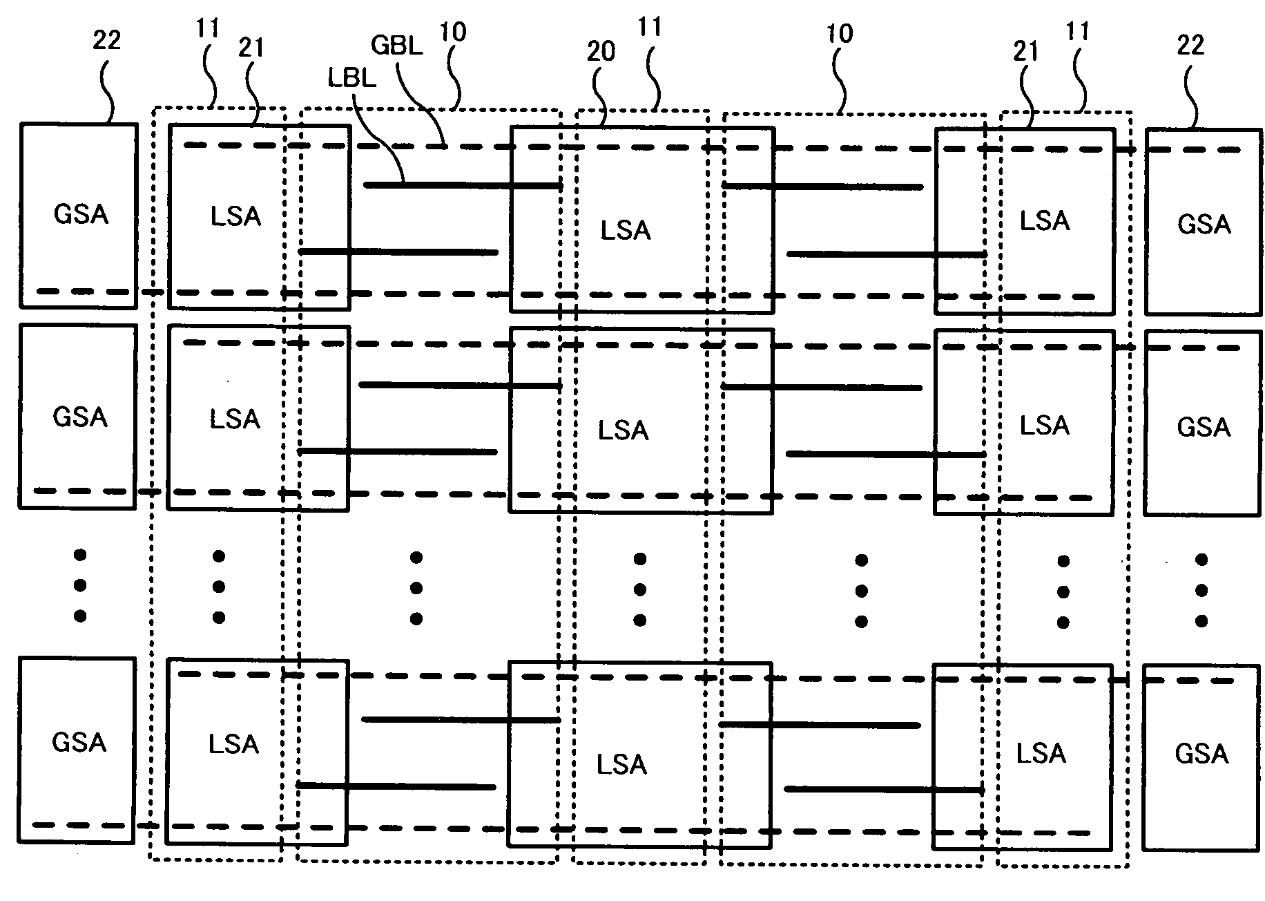
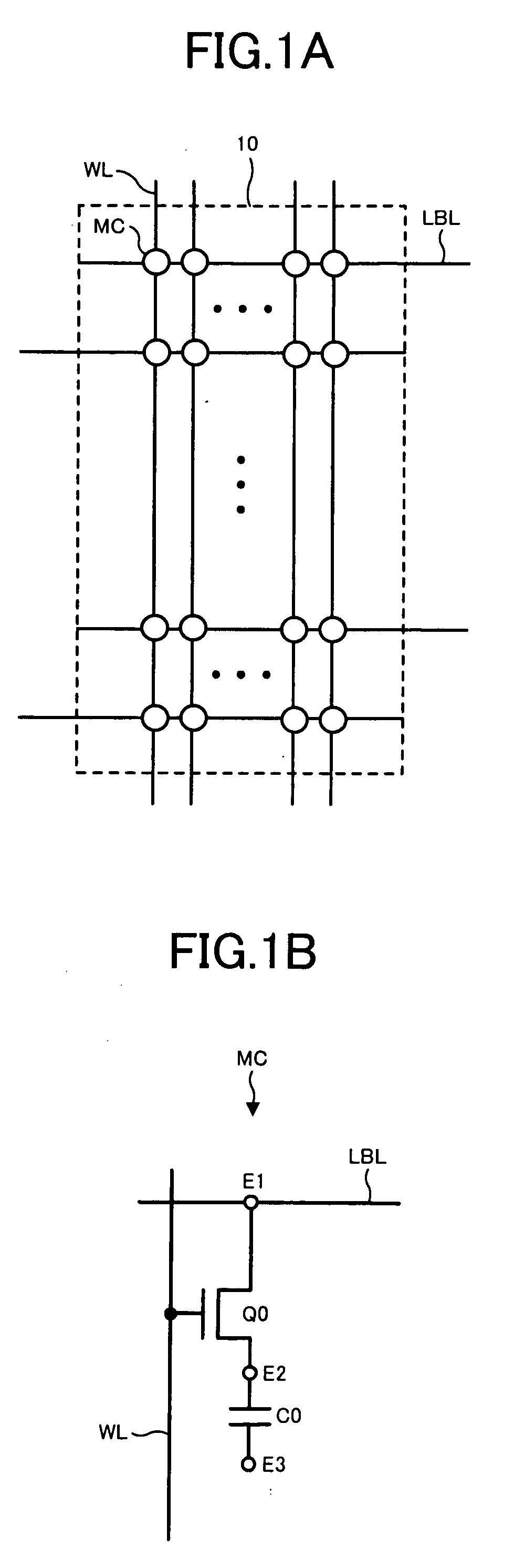
[0044]A first embodiment of the present invention will be described. In the first embodiment, the present invention is applied to DRAM as a semiconductor memory device, and a memory cell array is configured in which the vertical MOS transistor is employed as a select transistor of each memory cell. A configuration of the memory cell array of the first embodiment will be described with reference to FIG. 1A. As shown in FIG. 1A, in the memory cell array of the first embodiment, a plurality of word lines WL and a plurality of local bit lines LBL intersecting therewith are arranged in a memory cell array region 10, and there are provided a large number of memory cells MC (indicated by white circles) formed at intersections of the lines. For example, when M local bit lines LBL and N word lines WL are arranged in the memory cell array region 10, M×N memory cells MC are arranged in total so that the memory cell array having a storage capacity of M×N bits can be configured. Besides, the ver...

Example

Second Embodiment

[0071]Next, a second embodiment of the present invention will be described. The second embodiment is the same as the first embodiment in that the present invention is applied to DRAM as the semiconductor memory device and that the vertical MOS transistor is employed as the select transistor of the memory cell, however the hierarchy structure of the memory cell array differs from that of the first embodiment. Here, the configuration of the memory cell array of FIG. 1 is also common to the second embodiment, so description thereof will be omitted.

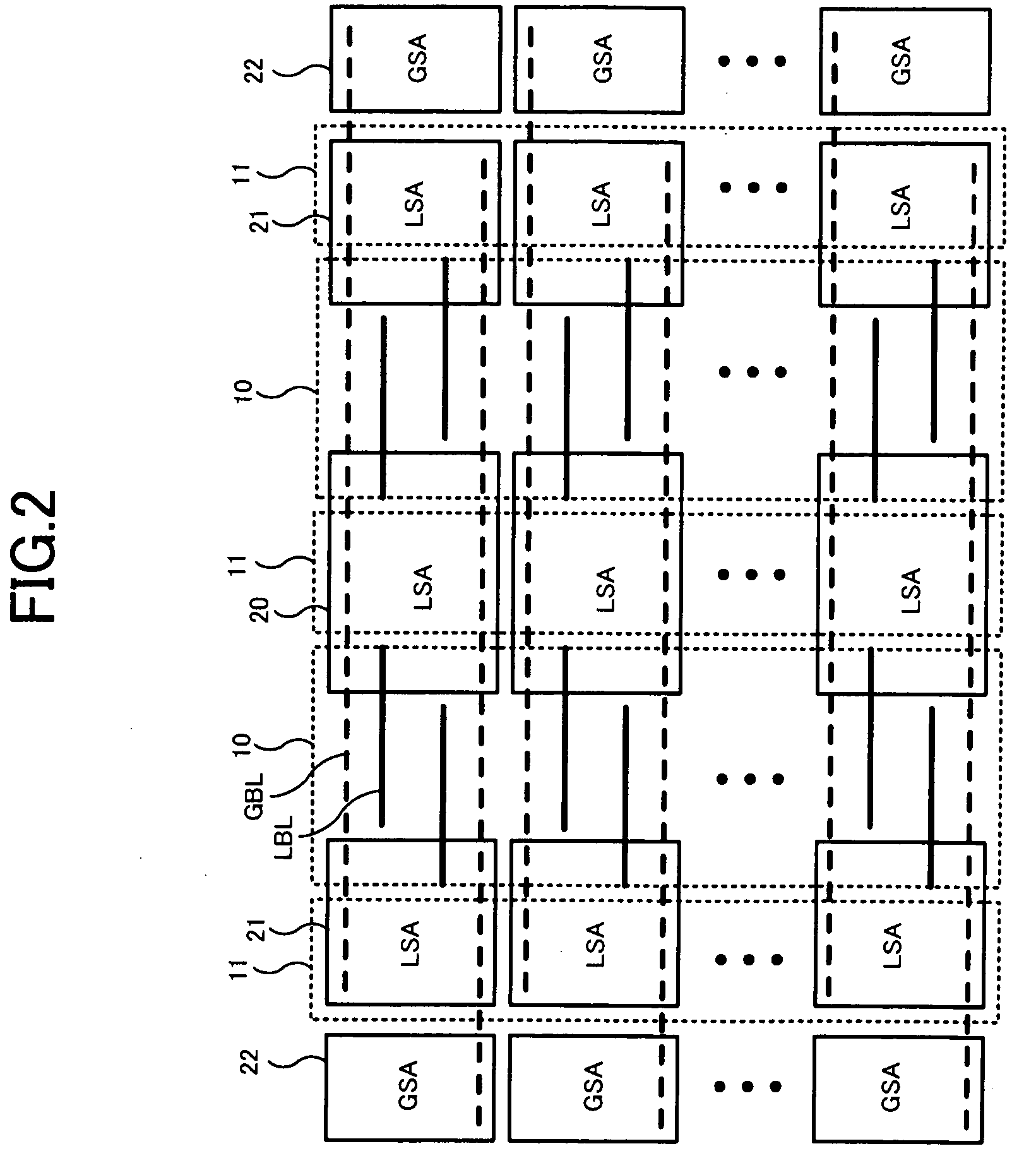
[0072]An entire configuration of DRAM of the second embodiment will be described with reference to FIG. 13. In FIG. 13, an inside area of a DRAM chip is partitioned into memory cell array regions 30 and peripheral circuit regions 31 in the same manner as in FIG. 2. The memory cell array of FIG. 1 is configured in each memory cell array region 30. In contrast, the local sense amplifiers 20 and 21 shown in FIG. 2 are not arran...


PUM


Abstract

A semiconductor memory device includes a memory cell array region in which vertical transistors each having a lower electrode connected to a bit line is regularly arranged with a predetermined pitch, including memory cells formed using at least the vertical transistors; a peripheral circuit region arranged adjacent to the memory cell array region in a bit line extending direction; and a predetermined circuit arranged overlapping the peripheral circuit region and the memory cell array region. In the semiconductor memory device, the vertical transistors each having an upper electrode connected to the predetermined circuit are included in an end region of the memory cell array region, in which no word line is provided.

Description

BACKGROUND OF THE INVENTION[0001]1. Field of the Invention[0002]The present invention relates to a semiconductor memory device which rewritably stores data in a plurality of memory cells formed at intersections of a plurality of word lines and a plurality of bit lines, and particularly relates to a semiconductor memory device employing an embedded bit line structure in which a bit line is arranged below a vertical transistor formed at each memory cell.[0003]2. Description of Related Art[0004]In order to reduce the chip area of a semiconductor memory device such as SRAM or DRAM, it is important to reduce an occupied area of a peripheral circuit disposed adjacent to a memory cell array, as well as to reduce an area of the memory cell array itself. Therefore, various layout methods for reducing the occupied area of the peripheral circuit such as sense amplifiers in the semiconductor memory device have been proposed (see Patent References 1 to 4). Also, in connection with these layout m...

Claims


Application Information

Patent Timeline
IPC IPC(8): G11C5/06G11C11/24G11C7/00
CPCG11C5/025G11C11/4097H01L27/0207G11C5/06H01L27/10876H01L27/10897H01L27/1052H01L27/105H10B99/00H10B12/50H10B12/053
Inventor KAJIGAYA, KAZUHIKO
Owner LONGITUDE LICENSING LTD
Why Eureka
Try Eureka