Curing methods for silicon dioxide thin films deposited from alkoxysilane precursor with harp ii process

a technology of alkoxysilane and curing method, which is applied in the direction of semiconductor/solid-state device manufacturing, basic electric elements, electric apparatus, etc., can solve the problems of large height-to-width gap, fabrication problem, and difficulty in completely filling gaps and trenches in these structures without creating

Inactive Publication Date: 2009-03-05
APPLIED MATERIALS INC
View PDF98 Cites 454 Cited by
  • Summary
  • Abstract
  • Description
  • Claims
  • Application Information

AI Technical Summary

Problems solved by technology

However, the vertical heights of the STIs normally do not decrease as fast as their horizontal widths, resulting in gaps and trenches with larger ratios of height to width (i.e., higher the aspect ratios).
While the ability to make device structures with increasing aspect ratios allows more of the structures (e.g., transistors, capacitors, diodes, etc.) to be packed onto the same surface area of a semiconductor chip substrate, it has also created fabrication problems.
One of these problems is the difficulty of completely filling the gaps and trenches in these structures without creating a void or seam during the filling process.
As aspect ratios increase, it becomes more difficult to fill deep narrow trenches without creating a void or seam in the dielectric material that fills the trench.
Voids and seams in a dielectric layer cause problems both during semiconductor device fabrication and in the finished devices.
This results in unpredictable and inconsistent post-deposition processing of the layer, such as uneven etching, polishing, annealing, etc.
This can result in erratic and inferior device performance due to electrical crosstalk, charge leakage, and in some instances, shorting within the device, among other problems.
A more conformal deposition can reduce material buildup at the top of the trench and the chance of dielectric material prematurely sealing off the top of the trench to form a void (a problem sometimes referred to as “breadloafing”).
Unfortunately however, slowing the deposition rate also means increasing the deposition time, which reduces processing efficiency and production rates.
However, increasing the flowability of an silicon oxide dielectric material by such conventional SOG films often results in an as-deposited film with low film density caused by residual carbon and silanol groups.
However, the high-temperature annealing used to remove residual carbon and OH groups may also cause a considerable degree of volumetric shrinkage of film.

Method used


Image

  • Curing methods for silicon dioxide thin films deposited from alkoxysilane precursor with harp ii process
  • Curing methods for silicon dioxide thin films deposited from alkoxysilane precursor with harp ii process
  • Curing methods for silicon dioxide thin films deposited from alkoxysilane precursor with harp ii process

Examples


Embodiment Construction

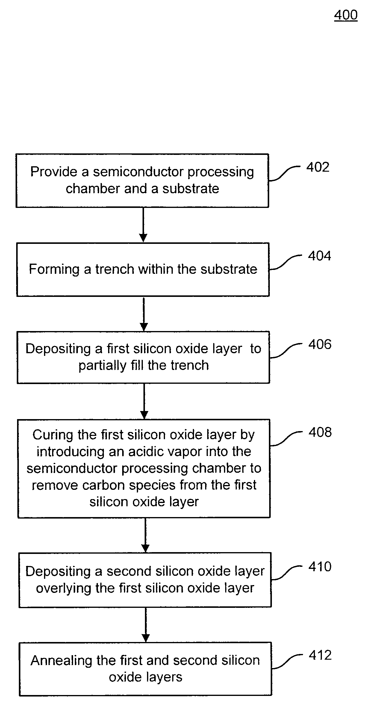
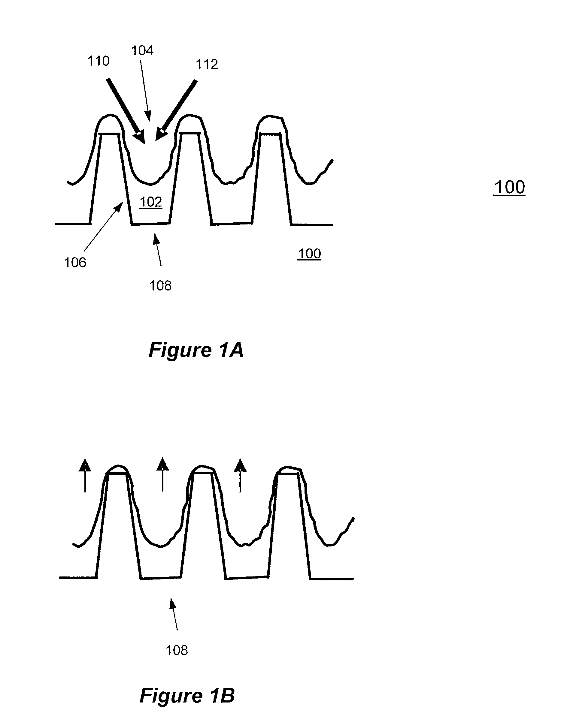
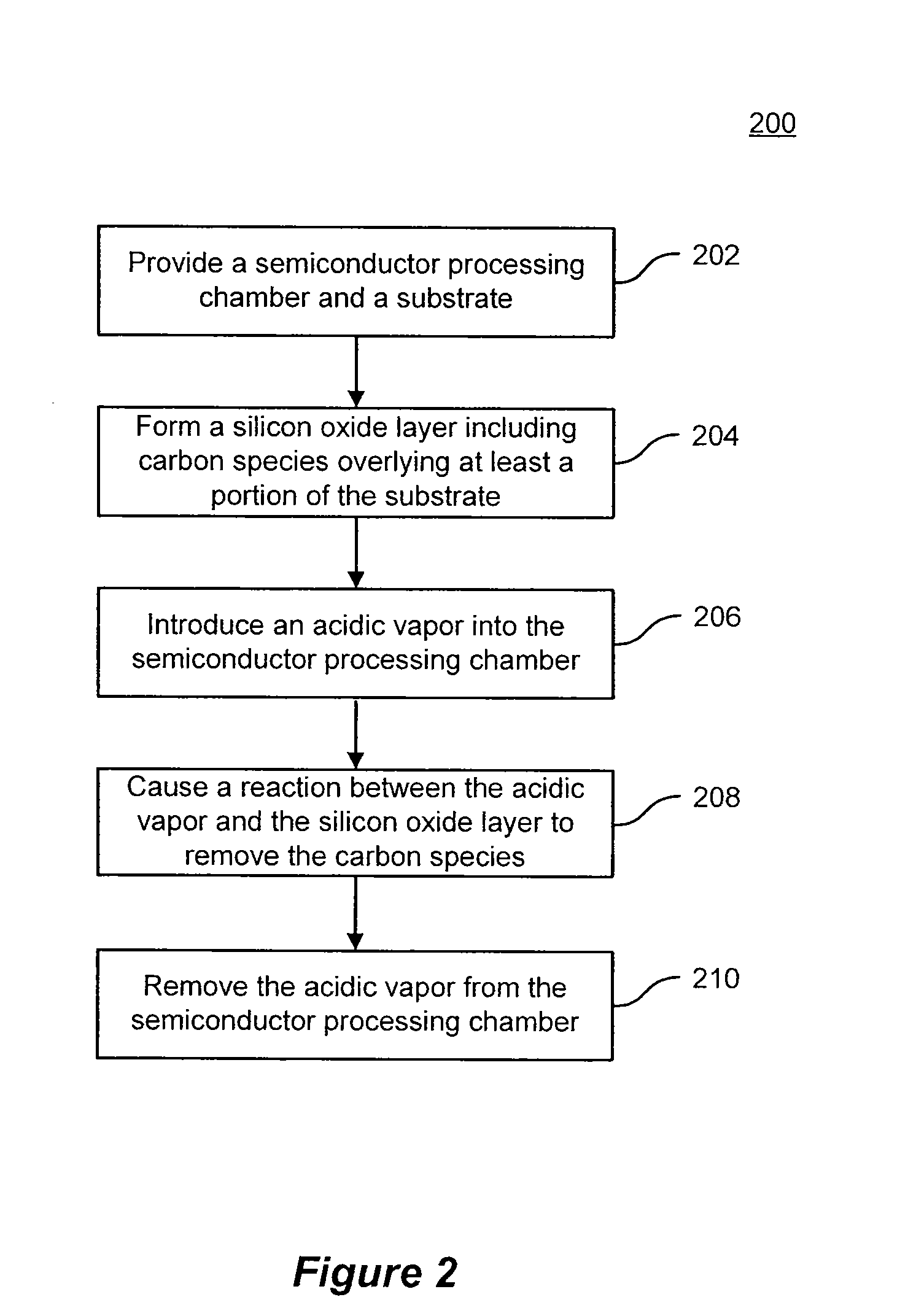
[0023]Systems and methods are described for curing a silicon layer with high flowability using an acidic catalyst to complete reactions in the as-deposited layer. Unwanted, residual species such as unreacted carbon groups present as a byproduct of the silicon layer deposition process can be removed from the silicon layer by curing the as-deposited silicon layer with an acidic catalyst. The catalyst aids in the removal of the unreacted carbon groups by helping to complete reactions in the as-deposited layer. The curing process allows for dense silicon oxide films having an improved wet etch ratio and gap fill capability for high aspect ratio trenches.

[0024]The methods of the invention include generating the acidic catalyst as an acidic, aqueous vapor. The acidic catalyst may be introduced directly into the semiconductor processing chamber as a gas such as hydrogen chloride (HCl) or generated in situ by using different precursors such as chloro-siloxane or acetoxy-siloxane. The additi...


PUM

PropertyMeasurementUnit
atmospheric pressureaaaaaaaaaa
temperatureaaaaaaaaaa
vapor pressureaaaaaaaaaa

Abstract

Methods of curing a silicon oxide layer on a substrate are provided. The methods may include the processes of providing a semiconductor processing chamber and a substrate and forming an silicon oxide layer overlying at least a portion of the substrate, the silicon oxide layer including carbon species as a byproduct of formation. The methods may also include introducing an acidic vapor into the semiconductor processing chamber, the acidic vapor reacting with the silicon oxide layer to remove the carbon species from the silicon oxide layer. The methods may also include removing the acidic vapor from the semiconductor processing chamber. Systems to deposit a silicon oxide layer on a substrate are also described.

Description

CROSS-REFERENCES TO RELATED APPLICATIONS[0001]This application is related to co-assigned U.S. patent application having attorney docket number A010498 / T69600, by Ingle et al, and titled “CHEMICAL VAPOR DEPOSITION OF HIGH QUALITY FLOW-LIKE SILICON DIOXIDE USING A SILICON CONTAINING PRECURSOR AND ATOMIC OXYGEN”, filed on May 30, 2006. This application is also related to co-assigned U.S. patent application having attorney docket number A11125 / T79600, by Munro et al, and titled “CHEMICAL TREATMENTS FOR IMPROVEMENT OF OXIDE FILM QUALITY.” This application is additionally related to co-assigned U.S. patent application having attorney docket number A1161 / T78800, by Mallick et al, and titled “HIGH QUALITY SILICON OXIDE FILMS BY REMOTE PLASMA CVD FROM DISILANE PRECURSORS.” The entire contents of both related applications is hereby incorporated by reference for all purposes.BACKGROUND OF THE INVENTION[0002]Gaps and trenches such as shallow trench isolation structures (STIs) are commonly emplo...

Claims


Application Information

Patent Timeline
Patent Type & Authority Applications(United States)
IPC IPC(8): H01L21/31
CPCH01L21/02126H01L21/02164H01L21/31633H01L21/3105H01L21/31608H01L21/02337
Inventor MALLICK, ABHIJIT BASUNEMANI, SRINIVAS D.WEIDMAN, TIMOTHY W.
Owner APPLIED MATERIALS INC
Why Eureka
Try Eureka