Optical near-field distribution transfer device

a transfer device and optical near-field technology, applied in the direction of optical elements, scanning probe techniques, instruments, etc., can solve the problems of limiting resolution, difficult to obtain a spatial resolution exceeding wavelength order by means of a usual microscopical technique, and nsom is not suitable for the use of transfer, etc., to achieve the effect of exceeding the limit of resolving power

Inactive Publication Date: 2009-03-12
RIKEN
View PDF3 Cites 7 Cited by
  • Summary
  • Abstract
  • Description
  • Claims
  • Application Information

AI Technical Summary

Benefits of technology

[0017]In other words, the invention utilizes the oscillation of electrons (localized plasmon) in the axial direction of small rods composed of a metal nanostructure made of, for example, a silver column having a diameter of a nanometer order, so that the image information having a limit of resolution being far below a wavelength can be transferred by means of the small rods. Thus, the invention contributes considerably to developments for a novel applied technology of light in a nanometer region.
[0018]In addition, although it has been considered heretofore that a nanomaterial is limited to carbon-base or semiconductor-base, or organic molecular materials, it becomes clear by the invention that a metal nanostructure is one of dominant nanomaterials.
[0019]In the following, the principle of the invention will be described for the sake of understanding easily the invention. The invention makes the transfer of image possible with exceeding the limit of resolving power due to wave properties of light. For instance, the invention is constituted in such that an array wherein columns each of which is made of silver and has a diameter of a nanometer order are disposed two-dimensionally (hereinafter referred optionally to as “two-dimensional metal nanocolumn array”) is used, whereby information can be transferred completely from the end on either side of the two-dimensional metal nanocolumn array to the end on the opposite side thereof in the axial direction over the limit of wavelength.
[0020]For instance, when an optical near-field is input to a columnar metal nanostructure made of silver and having a diameter of a nanometer order, localized surface plasmon polariton is induced on the surface of the metal nanostructure. In recent years, researches are actively conducted with respect to nanoimaging, nanolithography, plasmonic crystals and the like which use surface plasmon polariton; and they are attracted as a new field of research called nanoplasmonics.
[0021]Namely, there is the use of surface plasmon polariton (SPP) as one of promising method for confining a light in a region of a nanometer order in nanophotonics. The surface plasmon polariton is a condition wherein plasmon which is a mass oscillation phenomenon of free electrons inside a noble metal represented by gold (Au) or silver (Ag) becomes a propagating wave in a situation wherein the plasmon acts mutually with the outside light in the surface of the metal to be confined intensively inside the surface (see FIG. 1). If a metal is in small closed shape, for example, when it has a spherical or columnar shape having a diameter of several to several tens nm, the surface plasmon polariton combines easily with a light, so that the light can be confined into a small region. This is called by the name of localized surface plasmon polariton (see FIG. 2); and it is well known that the localized surface plasmon polariton scatters intensively the light of a particular color through the resonance to become a cause for coloring stained glass.
[0022]The present invention aims particularly at a mutual action of the phenomenon as described above with an optical near-field in small rods consisting of columnar materials each having a diameter of a nanometer order, for example, metal columnar small rods each having a diameter of a nanometer order (hereinafter referred optionally to as “metal nanocolumnar small rods”)

Problems solved by technology

However, there is such a problem that the limit of resolution due to wave properties of light in imaging wherein a conventional light is used.
As described above, it is difficult to obtain a spatial resolution exceeding wavelength order by means of a usual microscopical technique.
Consequently, the NSOM is not suitable for the use of the transfer of such information and applying a parallel processing therefor.
Accordingly, there are such problems that restrictions for an operating frequency, a film thickness condition of the metal film and the like are extremely severe, so that there are many technical difficulties in the actual application of lithography and the like; and further that an out-of-focus image is unavoidable due to the loss of a metal.
However, such a problem that there are many technical difficulties in the actual application of lithography in also this manner has been pointed out.

Method used


Image

  • Optical near-field distribution transfer device
  • Optical near-field distribution transfer device
  • Optical near-field distribution transfer device

Examples


Embodiment Construction

[0057]In the following, an example of embodiments of the optical near-field distribution transfer device according to the present invention will be described in detail by referring to the accompanying drawings.

[0058]First, FIG. 3 is a conceptual, structural, perspective view for explaining a first embodiment of the optical near-field distribution transfer device according to the present invention.

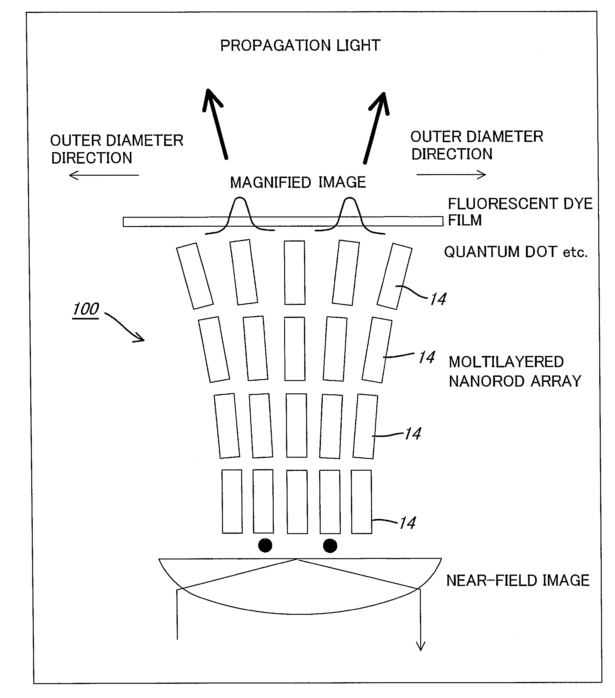
[0059]An optical near-field distribution transfer device 10 is constituted in such that a plurality of, for example, columnar solid small rods 14 made of silver (Ag), each of which has a diameter d of a nanometer order (e.g. 20 nm) and a length h in the axial direction (a height along Z-direction) of a nanometer order (e.g. 50 nm) in the surrounding medium 12 such as a dielectric material, and a semiconductor having a dielectric constant ∈d is “∈d≧1”, are erected at predetermined spacing g (the spacing g corresponds to a distance within which an electric field emerging from a small rod 14 d...


PUM

PropertyMeasurementUnit
sizeaaaaaaaaaa
thicknessaaaaaaaaaa
dielectric constant ∈maaaaaaaaaa

Abstract

Long-distance transfer of a super-resolution near field can be performed with a wavelength condition of high degree of freedom. Not only an image in same size can be merely transferred, but also a magnified image can be transferred. Thus the processing technique of a near-field image is improved. Small rods are erected at predetermined spacing with one another on a two-dimensional plane. At least the exterior surface of each small rod is made of a predetermined material having a dielectric constant ∈m meeting the condition “∈m≦−∈d” where ∈d is the dielectric constant of the surrounding medium. The axes of the small rods can be extended to a predetermined direction with respect to the two-dimensional plane. An optical near-field is incidented to one end of each small rod.

Description

TECHNICAL FIELD[0001]The present invention relates to an optical near-field distribution transfer device, and particularly to an optical near-field distribution transfer device which is used suitably in case of imaging a material.BACKGROUND TECHNOLOGY[0002]Heretofore, it has been known that light propagates in the atmosphere, light can transmit material information in a wide spectrum extending from ultraviolet to infrared, and light is a probe capable of imaging a material even in the atmosphere or water which is different from an electron microscope, and an atom force microscope.[0003]It is recognized that such imaging by the use of light is an extremely important technology in also a field of bioscience or the like wherein an observation of, for example, a live cell in a subwavelength level is required.[0004]However, there is such a problem that the limit of resolution due to wave properties of light in imaging wherein a conventional light is used. Namely, the resolution of an ima...

Claims


Application Information

Patent Timeline
Patent Type & Authority Applications(United States)
IPC IPC(8): G02F1/01
CPCB82Y15/00B82Y20/00G02B6/1226G01Q60/22G02B5/008B82Y35/00
Inventor KAWATA, SATOSHIKATO, JUN-ICHIONO, ATSUSHI
Owner RIKEN
Why Eureka
Try Eureka