Packaging substrate structure and method for manufacturing the same

a technology of packaging substrate and substrate structure, which is applied in the direction of conductive pattern formation, non-metallic protective coating application, and semiconductor/solid-state device details. it can solve the problems of inability to meet the requirements of conductivity. conventional wire bonding and other problems, to achieve the effect of improving the reliability of products, promoting quality of underfilling process, and reducing costs

Inactive Publication Date: 2009-03-19
PHOENIX PRECISION TECH CORP
View PDF6 Cites 12 Cited by
  • Summary
  • Abstract
  • Description
  • Claims
  • Application Information

AI Technical Summary

Benefits of technology

[0012]In view of the above-mentioned shortcomings of conventional techniques, the object of the present invention is to provide a packaging substrate structure and a method for manufacturing the same which can be applied to fin

Problems solved by technology

As performance of semiconductor processes is advanced, semiconductor chips formed thereby have more and stronger functions and tend towards complexity.
Inasmuch as chip techniques have developed towards high frequency and larger amounts of pins, conventional wire bonding has failed to satisfy demands of conductivity.
Although the structure on the surface of the packaging substrate 1 in FIG. 1 can be used for conduction, the solder bumps 14,14′ are not desirable in height and size due to difficulty in controlling those in a uniform quantity by coating or printing.
However, if the solder bumps 14,14′ are increased in height, costs are raised owing to increased amounts of solder materials.
Therefore, conventional structures and methods are not advantageous to fine bump pitch because of difficulty in controlling solder bumps to uniform height and size while forming solder bumps on solder pads.
Regarding the flip-chip structure c

Method used


Image

  • Packaging substrate structure and method for manufacturing the same
  • Packaging substrate structure and method for manufacturing the same
  • Packaging substrate structure and method for manufacturing the same

Examples


Embodiment Construction

[0028]Because of the specific embodiments illustrating the practice of the present invention, a person having ordinary skill in the art can easily understand other advantages and efficiency of the present invention through the content disclosed therein. The present invention can also be practiced or applied by other variant embodiments. Many other possible modifications and variations of any detail in the present specification based on different outlooks and applications can be made without departing from the spirit of the invention.

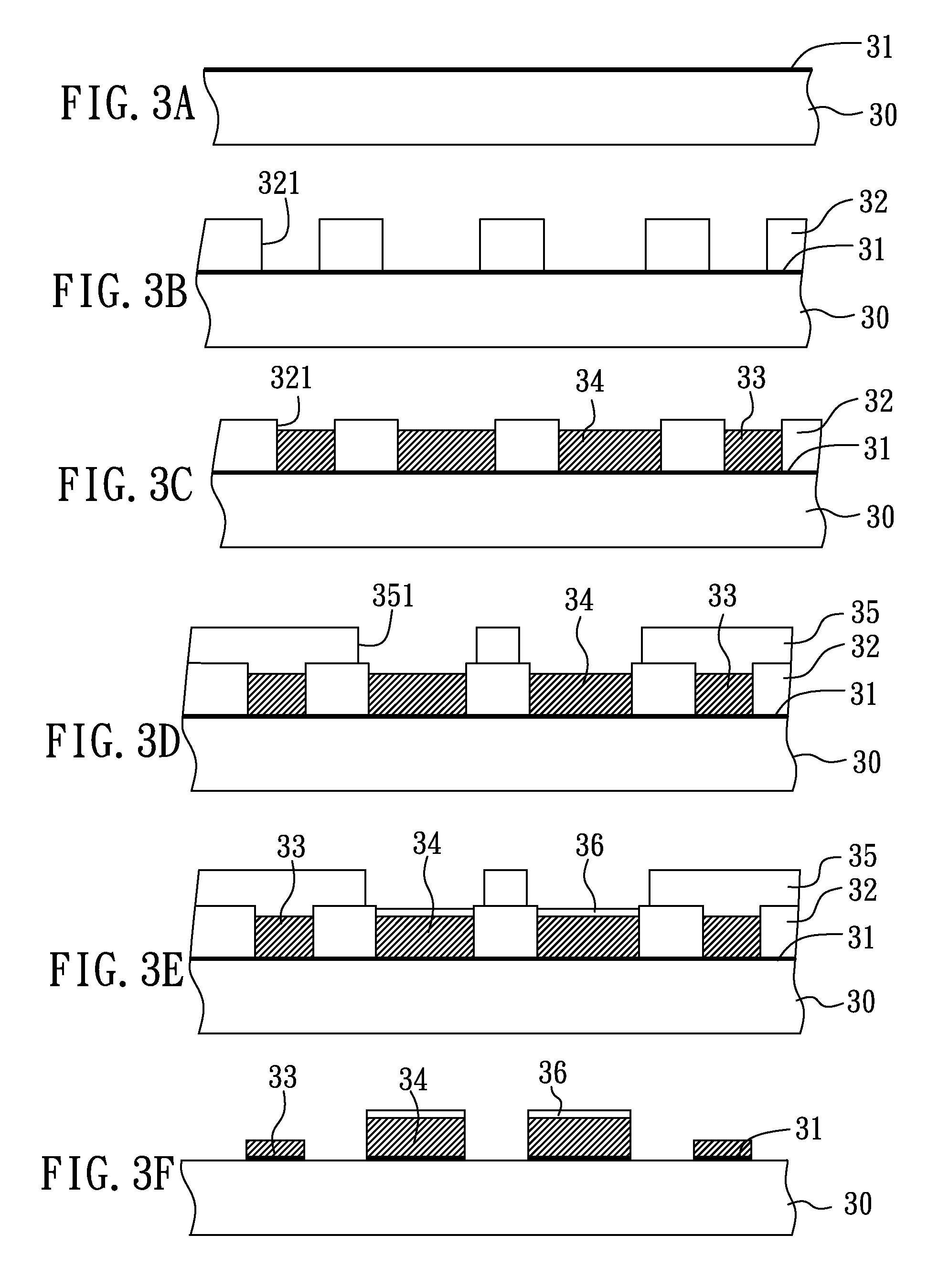
[0029]With reference to FIGS. 3A to 3I′, there is a flow chart in a cross-sectional view for manufacturing a packaging substrate structure in the present invention.

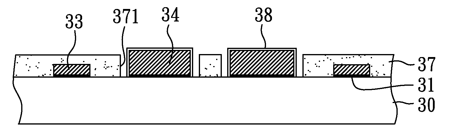
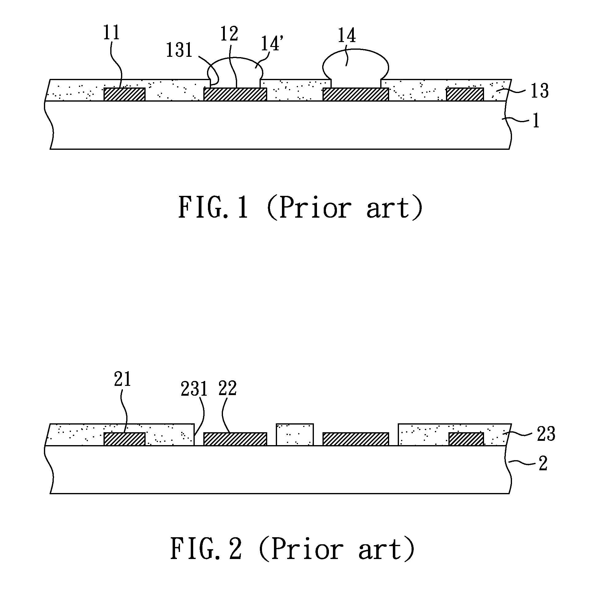
[0030]First, a substrate body 30 is provided as shown in FIG. 3A. A thin conductive layer 31 made of metal or nonmetal is formed on the surface of a dielectric layer of the substrate body 30.

[0031]As shown in FIG. 3B, a first resistive layer 32 is formed on the conductive layer 31. A plurality...


PUM

PropertyMeasurementUnit
Sizeaaaaaaaaaa
Electrical conductoraaaaaaaaaa

Abstract

The present invention relates to a packaging substrate and a method for manufacturing the same. The packaging substrate comprises: a substrate body, wherein a surface thereof has a circuit layer comprising a plurality of circuits and a plurality of conductive pads, and the conductive pads are higher than the circuits; and an insulating protection layer disposed on the surface of the substrate body, wherein the insulating protection layer has a plurality of openings exposing the conductive pads, and the size of the openings is larger than or equal to that of the conductive pads. Accordingly, the packaging substrate structure of the present invention can be employed in a flip-chip packaging structure of fine-pitch.

Description

BACKGROUND OF THE INVENTION[0001]1. Field of the Invention[0002]The present invention relates to a packaging substrate structure and a method for manufacturing the same, and, more particularly, to a packaging substrate structure suitable for application in a flip-chip packaging structure having fine pitch and a method for manufacturing the same.[0003]2. Description of Related Art[0004]As performance of semiconductor processes is advanced, semiconductor chips formed thereby have more and stronger functions and tend towards complexity. At the same time, amounts of transmission data of semiconductors increase more and more. Therefore, pins of semiconductors have to increase in accordance with the above-mentioned.[0005]Inasmuch as chip techniques have developed towards high frequency and larger amounts of pins, conventional wire bonding has failed to satisfy demands of conductivity. Compared with conventional wire bonding, a flip-chip process is a technique that a chip faces downward to...

Claims


Application Information

Patent Timeline
IPC IPC(8): H05K1/09H05K3/10
CPCH01L23/498Y10T29/49165H01L24/81H01L2224/1147H01L2224/11901H01L2224/81801H01L2924/01029H01L2924/01033H01L2924/01079H01L2924/01082H05K3/062H05K3/108H05K3/28H05K3/4007H05K2201/0367H05K2201/09736H05K2201/10674H05K2203/0361H05K2203/0369H05K2203/0574H01L2924/01006H01L2924/01024H01L2924/01047H01L2924/0105H01L2224/11902H01L24/14H01L2224/1403H01L23/49822H01L23/12
Inventor HSU, SHIH-PING
Owner PHOENIX PRECISION TECH CORP
Why Eureka
Try Eureka