Semiconductor device and its manufacturing method

a technology of semiconductor devices and semiconductor films, applied in semiconductor devices, capacitors, electrical devices, etc., can solve the problems of difficult uniform etching of hydrogen barrier films, interlayer dielectric films may have differences in thickness, and ferroelectric films may possibly be deteriorated, etc., to achieve uniform thickness, high accuracy of shape, and favorable formation

Active Publication Date: 2009-03-19
SEIKO EPSON CORP
View PDF9 Cites 30 Cited by
  • Summary
  • Abstract
  • Description
  • Claims
  • Application Information

AI Technical Summary

Benefits of technology

[0021]As the stopper film is formed from a dielectric material having a smaller etching rate than that of the interlayer dielectric film, the stopper film can be functioned as an etching stopper at the time of etching the interlayer dielectric film in the step of forming a contact hole. Therefore, even when the etching is excessively conducted in consideration of differences in the thickness of the interlayer dielectric film, the differences in the thickness of the interlayer dielectric film are not reflected in the thickness of the stopper film, and therefore the stopper film can be uniformly etched. As a result, the hydrogen barrier film has a uniform thickness, and thus can be processed in a highly accurate shape, such that the inner wall surface of the contact hole at the hydrogen barrier film can be processed in a desired shape, more specifically, a shape in which the inner wall surf

Problems solved by technology

However, if the measures are not sufficient against the reducing atmosphere at the time of forming the plugs over the ferroelectric capacitor in the methods described in the aforementioned patent documents, the ferroelectric film may possibly be deteriorated.
However, due to differences in the thickness of the film at the time of film formation and in the polishing amount caused by unevenness in the base layer, the interlayer dielectric film may have differences in its thickness.
For this reason, when forming contact holes by etching the interlayer dielectric film and the hydrogen barrier film, the differences in the thickness of the interlayer dielectric film are reflected in the hydrogen barrier film, which makes it difficult to uniformly etch the hydrogen barrier film.
As a result, the side wall of the hydrogen ba

Method used


Image

  • Semiconductor device and its manufacturing method
  • Semiconductor device and its manufacturing method
  • Semiconductor device and its manufacturing method

Examples


Embodiment Construction

[0028]An embodiment of the invention is described below with reference to the accompanying drawings. However, it should be noted that the technical scope of the invention is not limited to the embodiment described below. Although various structures may be exemplified in the following description, using the accompanying drawings, the measurement and scale of each of the components of the structures illustrated in the drawings may be appropriately changed with respect to the actual structures so that characteristic features of each of the structures can be readily recognized.

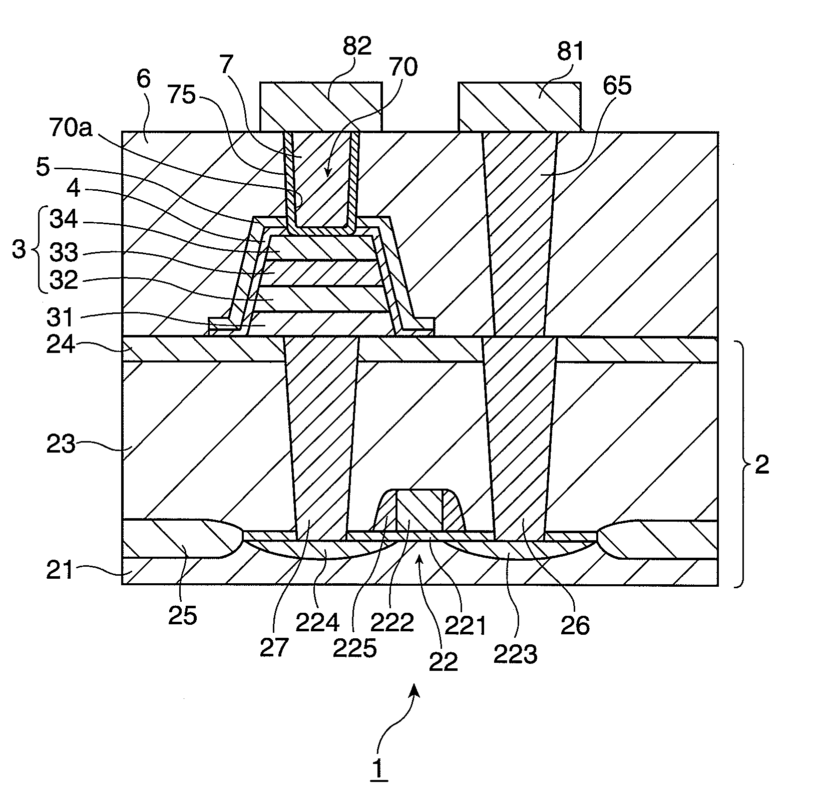
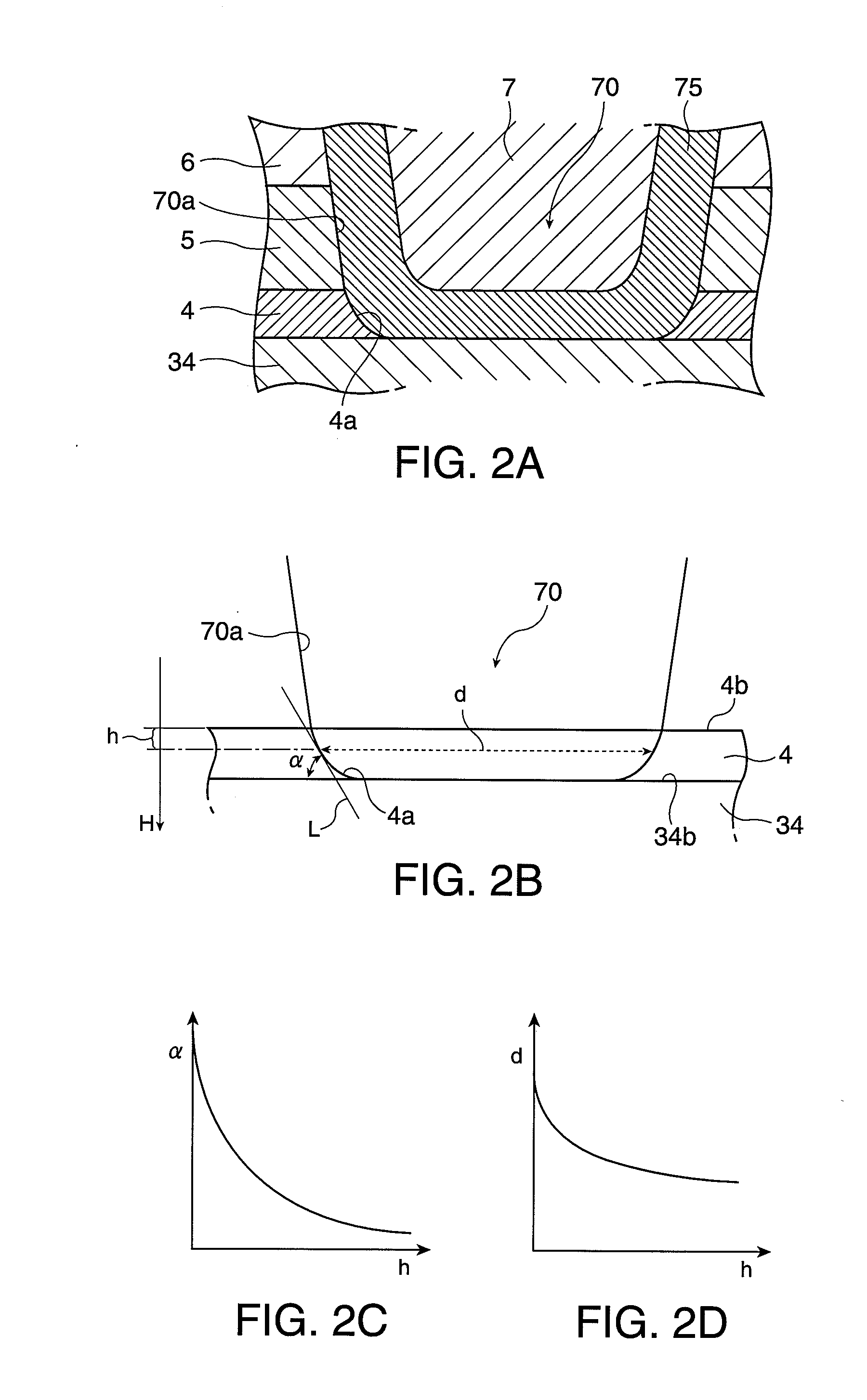
[0029]FIG. 1 is a cross-sectional view of the structure of a main portion of a semiconductor device (ferroelectric memory device) 1 in accordance with an embodiment of the invention. As shown in FIG. 1, the ferroelectric memory device 1 has a stacked type structure, and is equipped with a ferroelectric capacitor 3 provided on a base substrate 2, a hydrogen barrier film 4 that covers a top surface and a side surfac...


PUM


Abstract

A semiconductor device includes: a ferroelectric capacitor including a first electrode provided above a substrate, a ferroelectric film provided on the first electrode and a second electrode provided on the ferroelectric film; a hydrogen barrier film that covers a top surface and a side surface of the ferroelectric capacitor; an interlayer dielectric film that covers the ferroelectric capacitor and the substrate; a contact hole that penetrates the interlayer dielectric film and the hydrogen barrier film and exposes the second electrode; a barrier metal that covers a top surface of the second electrode exposed in the contact hole and an inner wall surface of the contact hole and is composed of a conductive material having hydrogen barrier property; and a plug conductive section that is embedded in the contact hole and conductively connects to the barrier metal, wherein the inner wall surface of the contact hole at the hydrogen barrier film includes a concave curved surface facing the interior of the contact hole, and the contact hole at the hydrogen barrier film has an inner diameter that gradually becomes smaller toward the second electrode.

Description

[0001]The entire disclosure of Japanese Patent Application No. 2007-241017, filed Sep. 18, 2007 is expressly incorporated by reference herein.BACKGROUND[0002]1. Technical Field[0003]The present invention relates to semiconductor devices, and also relates to methods for manufacturing the same.[0004]2. Related Art[0005]Ferroelectric memory devices (FeRAM) are nonvolatile memories capable of low voltage and high speed operations, and their memory cells can be each formed from one transistor and one capacitor (1T / 1C). Accordingly, ferroelectric memory devices can achieve integration at the same level of that of DRAM, and are therefore expected as large-capacity nonvolatile memories.[0006]As the structures of such ferroelectric memory devices, a planer type (see, for example, Japanese laid-open patent application JP-A-2003-347512) and a stacked type (see, for example, Japanese laid-open patent application JP-A-2006-310637) may be enumerated. A ferroelectric memory device in either of the...

Claims


Application Information

Patent Timeline
IPC IPC(8): H01L21/02H01L27/11
CPCH01L27/11502H01L28/57H01L27/11507H10B53/30H10B53/00
Inventor NODA, TAKAFUMI
Owner SEIKO EPSON CORP
Why Eureka
Try Eureka