

Laser decal transfer of electronic materials
a technology of electronic materials and laser decals, applied in the direction of transfer patterning, coating, printed circuit repair/correction, etc., can solve the problems of limited material choice, slow deposition speed, limited success of techniques, etc., to dampen any shear force, high viscosity, and high uniform thickness and morphology
- Summary
- Abstract
- Description
- Claims
- Application Information
AI Technical Summary
Benefits of technology
Problems solved by technology
Method used
Image

Examples
Embodiment Construction
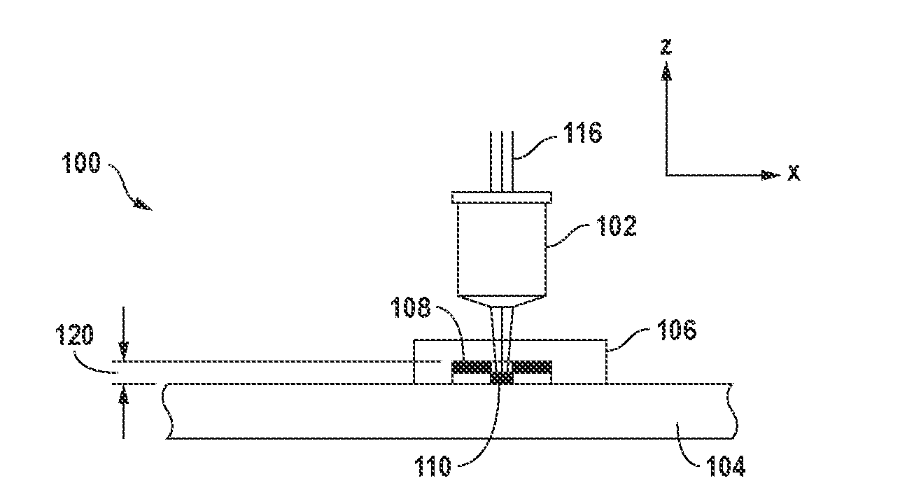
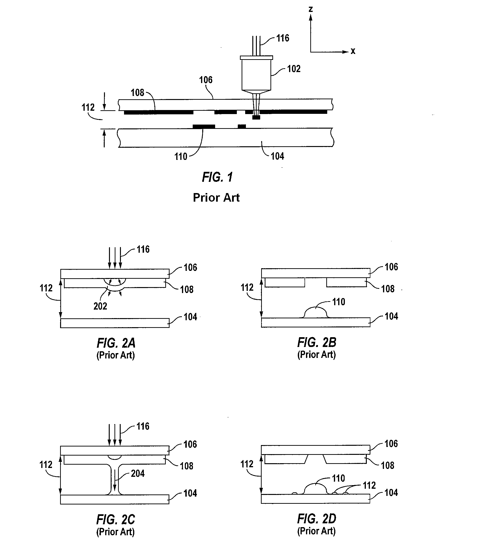
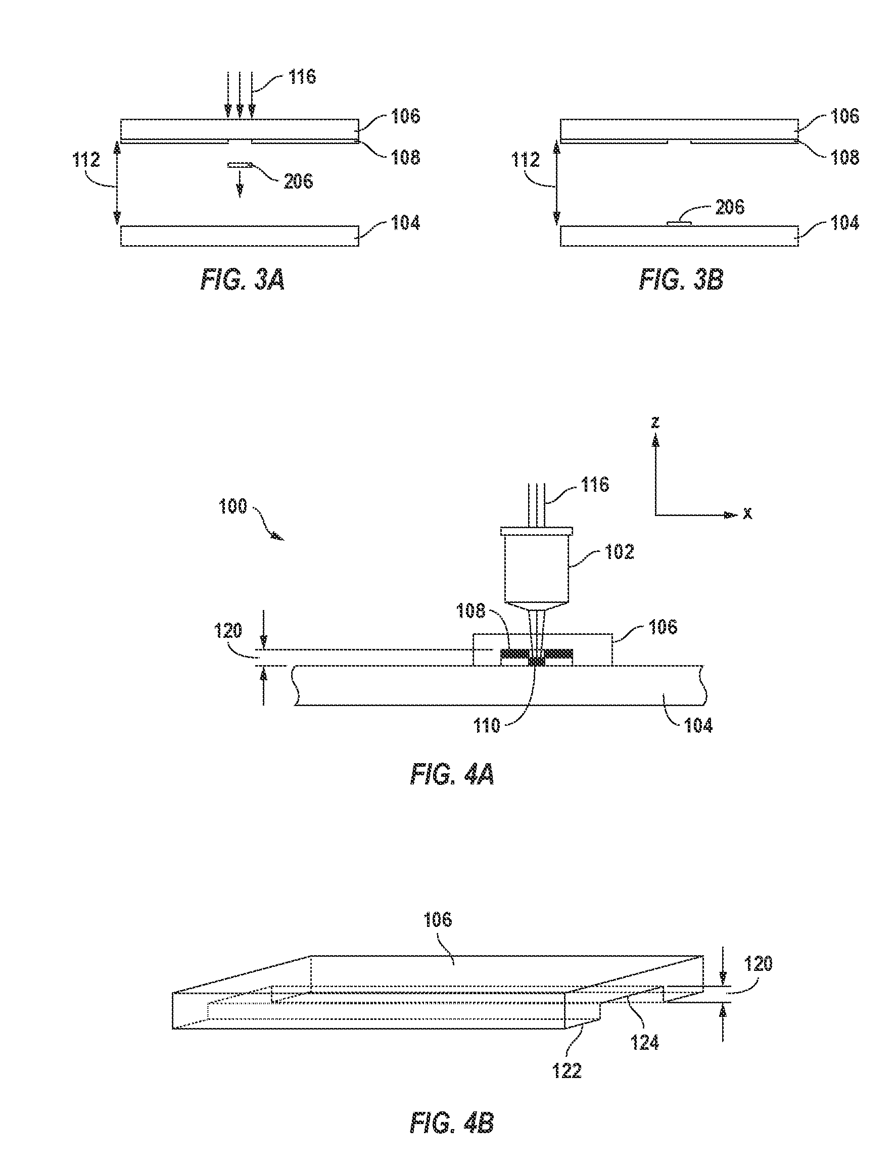
[0032]In accordance with one embodiment of the present invention, a rheological compound with a defined shape is transferred from a target substrate to a receiving substrate using an incident laser beam. The compound is illuminated with a laser beam whose energy density is so selected as to cause a decal transfer of the laser-illuminated non-evaporated rheological compound to occur. Accordingly, the laser-illuminated non-evaporated rheological compound is released from and propelled away from the target substrate and is deposited at a defined location on the receiving substrate.
[0033]The decal transfer, also called template transfer, in accordance with the present invention, achieves the desired small line widths and sub-micrometer thicknesses. More specifically, the decal transfer is a transfer of rheological material that has substantially one-to-one correspondence in shape and area to the laser transferring pulse striking the target substrate, i.e., ribbon, on which the material ...
PUM
| Property | Measurement | Unit |
|---|---|---|
| thickness | aaaaa | aaaaa |
| thickness | aaaaa | aaaaa |
| thickness | aaaaa | aaaaa |
Abstract
Description
Claims
Application Information