Flexible on chip testing circuit for i/o's characterization

a testing circuit and flexible technology, applied in the direction of voltage-current phase angle, instruments, pulse characteristics measurement, etc., can solve the problems of high test cost, increased test duration, time-consuming and labor-intensive tests,

Active Publication Date: 2009-03-19
STMICROELECTRONICS PVT LTD
View PDF10 Cites 10 Cited by
  • Summary
  • Abstract
  • Description
  • Claims
  • Application Information

AI Technical Summary

Benefits of technology

[0009]It is an object of the present invention to provide a flexible on-chip testing circuit for characterization of I / O pin parameters on a plurality of I / O structures.

Problems solved by technology

Since fabrication complexities have increased, hence tests have to be targeted not only to debug design related issues but also process related ones as considerable process spread is observed in newer technologies.
Such characterization test would require a sophisticated expensive tester and also increase test duration if the tests are performed manually.
Although commercial on-chip test solutions exist for other macros, most of the tests done today for the measurement of I / O pin parameters starting from the application of test patterns to the observation and compilation of results are manual thus making the tests, time intensive and prone to instrument errors.
Moreover characterization tests are performed on a few packaged dies, which do not guarantee design robustness with process spread.
This would require a very sophisticated tester thus enormously adding to the cost of test.

Method used


Image

  • Flexible on chip testing circuit for i/o's characterization
  • Flexible on chip testing circuit for i/o's characterization
  • Flexible on chip testing circuit for i/o's characterization

Examples


Embodiment Construction

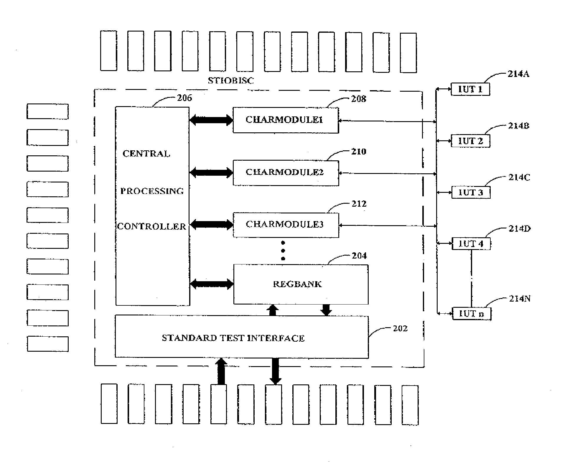
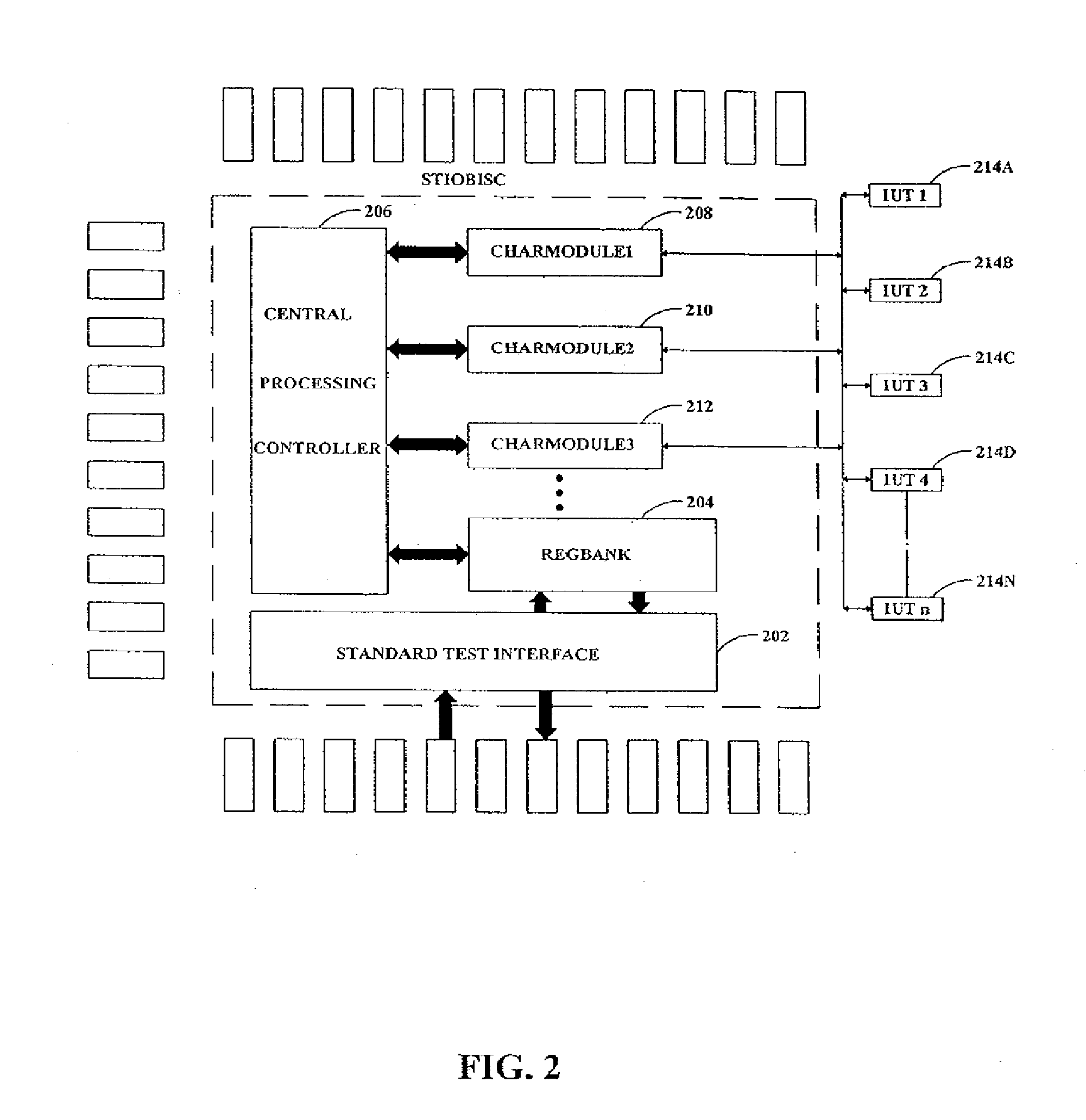
[0034]The present invention provides a cost-effective and flexible circuit and corresponding method for on-chip testing for I / O characterizations of different types of input and output I / O structures. The invention provides a flexible circuit for characterizing the pin parameters of I / O structures for a multi-voltage IUT, or a single voltage IUT.

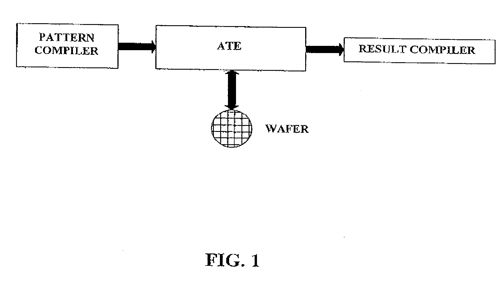
[0035]FIG. 1 illustrates a test setup of a flexible on-chip testing circuit for I / O characterization. A low speed and low cost Automatic test equipment (ATE) is used for generating the patterns required to initialize the setup for the logic inside the chip. STIOBISC can be used for I / O characterization at wafer level as well as package level. The ‘ASSEMBLER’ shown is a software program which gives an interactive and easy way to convert the patterns to be fed inside into required bit stream. The ‘RESULT COMPILER’ takes the output binary data from the ATE and converts them into the final test and characterization results, which can be directly...


PUM


Abstract

The present invention provides a flexible on-chip testing circuit and methodology for measuring I / O characterization of multiple I / O structures. The testing circuit includes a register bank, a central processing controller (CPC), a character slew module, a delay characterization module, and a character frequency module. The register bank stores multiple instructions, and measurement results. The CPC fetches the instructions from the register bank. The CPC includes various primary and secondary state machines for interpreting the fetched instructions for execution. Depending on the input instruction the CPC applies stimulus to the IUT and the output of the IUT is used by the Local characterization modules (CHARMODULE) to extract the desired characterization parameters such as the character slew module which measures a voltage rise / fall time either for a single voltage IUT or a multi-voltage IUT. The Test Methodology for STIOBISC consists of an automated ATE pattern generation from verification test benches and automated result processing by converting the ATE data logs into the final readable format, thereby considerably reducing the test setup and output processing time. The testing circuit can operate in multiple modes for selecting one of these modules.

Description

CROSS REFERENCE TO RELATED APPLICATIONS[0001]This application is a continuation of U.S. application Ser. No. 11 / 875,837, filed Oct. 20, 2007 Entitled FLEXIBLE ON CHIP TESTING CIRCUIT FOR I / O'S CHARACTERIZATION, which application is incorporated herein by reference in its entirety.BACKGROUND OF THE INVENTION[0002]1. Field of the Invention[0003]The present invention relates to chip testing circuits, and more specifically to a flexible on-chip testing circuit for I / Os characterization of different types of I / O structures.[0004]2. Discussion of the Related Art[0005]Input / Output (I / O) buffers are features of an integrated circuit which must be thoroughly tested because it is the I / O element which finally interfaces the core signal to the off-chip environment. The test of I / O circuitry involves measurement of various I / O pin DC and AC parameters. Since fabrication complexities have increased, hence tests have to be targeted not only to debug design related issues but also process related ...

Claims


Application Information

Patent Timeline
Patent Type & Authority Applications(United States)
IPC IPC(8): G01R31/317
CPCG01R31/31715
Inventor VIJAYARAGHAVAN, NARAYANANSINGH, BALWANT
Owner STMICROELECTRONICS PVT LTD
Why Eureka
Try Eureka