Circuit board structure with capacitor embedded therein and method for fabricating the same

a capacitor and circuit board technology, applied in the direction of printed capacitor incorporation, conductive pattern formation, non-printed electric components of printed circuits, etc., can solve the problems of signal interference, poor fluidity of high dielectric materials, and increased noise interference in package structures

Inactive Publication Date: 2009-03-26
PHOENIX PRECISION TECH CORP
View PDF0 Cites 6 Cited by
  • Summary
  • Abstract
  • Description
  • Claims
  • Application Information

AI Technical Summary

Benefits of technology

[0008]Another object of the present invention is to provide a structure in which the size precision of the electrode plate of the capacitor is enhanced as well as a method for fabricating the same.
[0009]Yet another object of the present invention is to provide a packaging substrate structure with fine lines.
[0017]In the present invention, the material of the buffer layer can be a photoimagable dielectric material. Preferably, the buffer layer of the present invention is made of a photoimagable dielectric material with low coefficient of thermal expansion (CTE) and low dielectric constant (Dk). In addition, the buffer layer of the present invention can be patterned by exposure and development to form a plurality of open areas. In comparison to the conventional method in which a wiring layer is formed and then high dielectric material is laminated thereon, the problem that voids occur in the process for depositing high dielectric material between circuits can be overcome by the method provided by the present invention, in which a buffer layer is formed and patterned to form open areas, and then a wiring layer is formed in the open areas. In addition, since the open areas of the buffer layer can be formed by exposure and development, the precision of the capacitor can be controlled accurately. Also, a structure with fine lines can be fabricated by controlling the size of the open areas of the buffer layer, and the problem that voids are generated in the process for depositing high dielectric material between circuits will not occur.
[0019]Besides, the circuit board structure with a capacitor embedded therein according to the present invention can further comprise a built-up structure, which can be a single-layered or multi-layered structure. Herein, the built-up structure can be formed on the second circuit layer. The built-up structure can include a dielectric layer, a wiring layer and conductive vias. The conductive vias can electrically connect each wiring layer of the built-up structure, or electrically connect to the outer wiring layer in the circuit board structure with a capacitor embedded therein. In addition, the circuit board structure with a capacitor embedded therein according to the present invention can further comprise a solder mask on the surface of the built-up structure to protect the circuit board structure.
[0020]Accordingly, in the circuit board structure with a capacitor embedded therein and the method for fabricating the same provided by the present invention, the gap between circuits can be filled with a buffer layer beforehand by forming a buffer layer, patterning the buffer layer to form open areas, and then forming a wiring layer in the open areas, so that problems such as void generation caused by the insufficient amount of binder in the high dielectric material and the excessively low thickness thereof can be solved. In addition, the leakage caused by the parasitic capacitance between circuits of the same wiring layer also can be inhibited. Furthermore, since the buffer layer is patterned by exposure and development to define the areas of the capacitor regions, the precision of the capacitor regions can be more accurately controlled in comparison to the conventional method in which the capacitor regions are defined by etching the wiring layer. Also, a structure with fine lines can be fabricated by controlling the size of the open areas of the buffer layer, and the problem that voids are generated in the process for depositing high dielectric material between circuits will not occur.

Problems solved by technology

However, owing to the increased number of I / O terminals and highly dense circuit layouts, noise interference in a package structure now becomes greater than it was before.
However, since the high dielectric material layer is filled with a large amount of ceramic material (60 vol % or more), it results in poor fluidity of the high dielectric material.
Due to the increased thickness of the circuits, the too-narrow gap between the circuits or the decreased thickness of the high dielectric material layer, voids inevitably occur during the filling process and result in trouble.
As a result, parasitic capacitance occurs between the circuits of the same wiring layer, and further results in signaling interference such as current leakage, especially in the application at high frequency.

Method used


Image

  • Circuit board structure with capacitor embedded therein and method for fabricating the same
  • Circuit board structure with capacitor embedded therein and method for fabricating the same
  • Circuit board structure with capacitor embedded therein and method for fabricating the same

Examples


embodiment 1

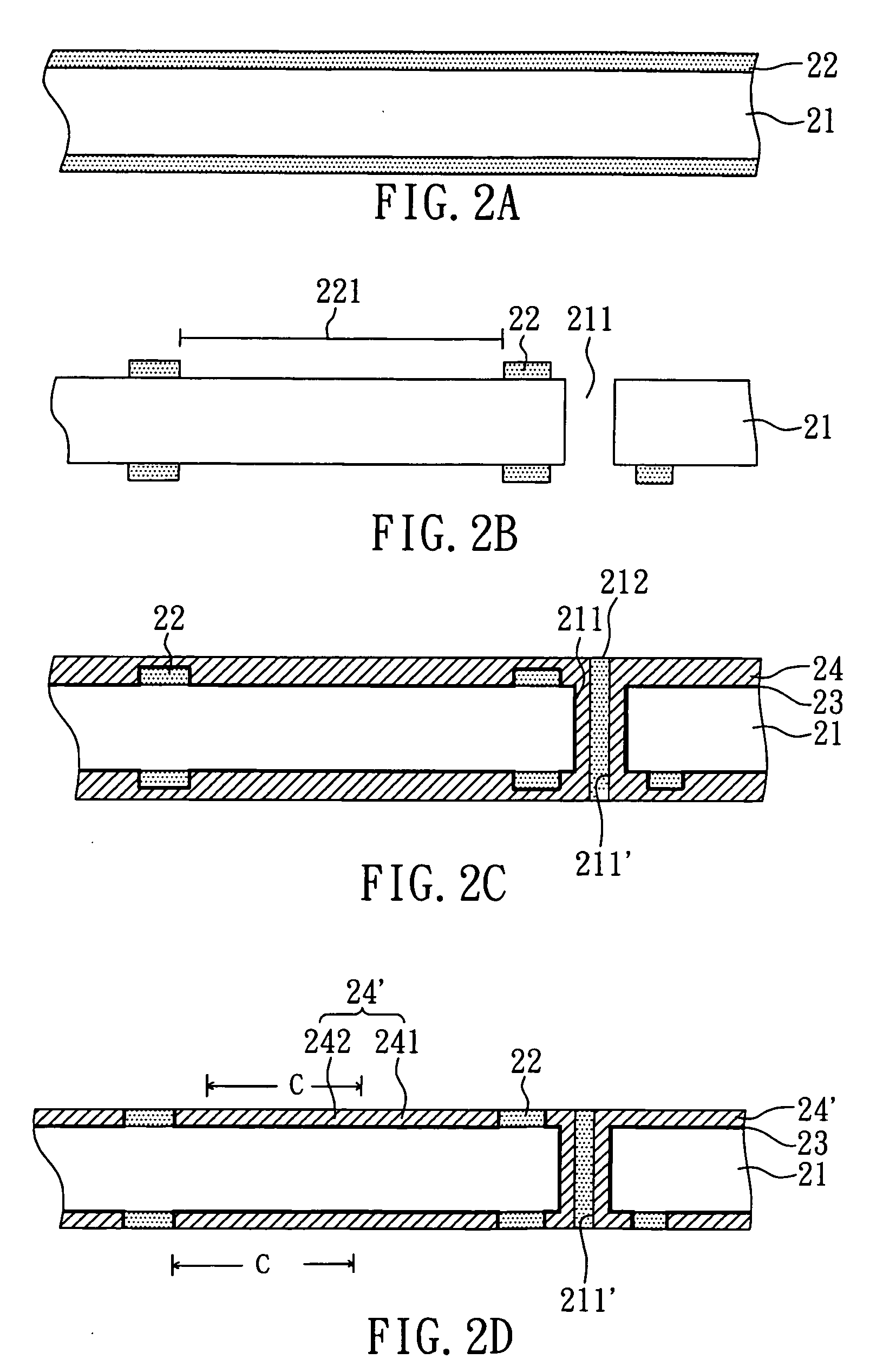
[0031]With reference to FIGS. 2A to 2F, there are shown cross-section views for illustrating a process of fabricating a circuit board structure with a capacitor embedded therein according to the present invention.

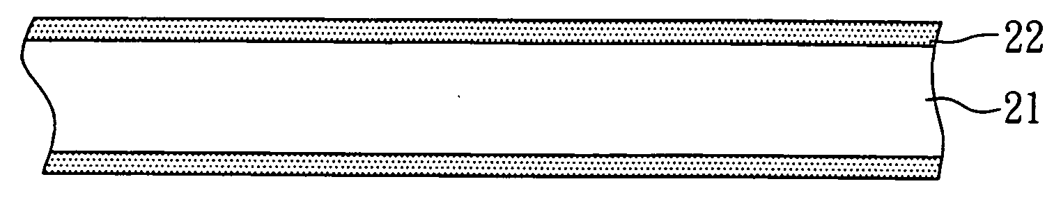
[0032]As shown in FIG. 2A, a core board 21 is first provided and then a buffer layer 22 is formed on two opposite surfaces of the core board 21 by one of coating, printing and attaching. Herein, the type of the core board 21 is not limited and can be an insulating board or a core board with inner circuits. In the present embodiment, the core board 21 is an insulating board, and the material of the buffer layer 22 is a photoimagable dielectric material.

[0033]Subsequently, as shown in FIG. 2B, an internal through hole 211 is formed in the core board 21 by laser ablation or mechanical drilling, and the buffer layer 22 is patterned by photolithography (i.e. exposure and development) to form a plurality of open areas 221.

[0034]As shown in FIG. 2C, a first seed layer 23 is formed...

embodiment 2

[0039]With reference to FIGS. 3A and 3B, there are shown cross-section views for illustrating a process of fabricating a circuit board structure with a capacitor embedded therein according to the present invention. The present embodiment is substantially similar to Embodiment 1, except that the via 251 is fully filled with conductive material in the process for forming the second metal layer 27 by electroplating, as shown FIG. 3A. Accordingly, the circuit board structure with a capacitor embedded therein, as shown in FIG. 3B, can be obtained by etching or the manner as shown in FIG. 2F′. As a result, the conductive via 251′ formed in the via 251 is fully filled with conductive material.

embodiment 3

[0040]With reference to FIG. 4, a built-up structure shown in FIG. 4 can be formed on the surface of the circuit board structure with a capacitor embedded therein as manufactured in Embodiment 1. As shown in FIG. 4, the built-up structure 30 includes a dielectric layer 31, a wiring layer 32 stacked on the dielectric layer 31, and conductive vias 33 formed in the process for forming the wiring layer 32. The wiring layer 32 and the conductive vias 33 can be formed by the following process. First, a seed layer (not shown in FIG. 4) is formed on the dielectric layer 31. Subsequently, a resist layer (not shown in FIG. 4) is applied over the dielectric layer 31 with the seed layer thereon and patterned (not shown in FIG. 4) by exposure and development. Finally, a metal layer such as Cu is formed by electroplating on the seed layer, and then the resist layer and the seed layer thereunder are removed so as to form the wiring layer 32 and the conductive vias 33. Herein, the conductive vias 3...


PUM

PropertyMeasurementUnit
dielectric constantaaaaaaaaaa
dielectricaaaaaaaaaa

Abstract

The present invention relates to a circuit board structure with a capacitor embedded therein and the method for fabricating the same. The disclosed structure comprises: a core board; a buffer layer disposed on two surfaces of the core board and having a plurality of open areas; a first circuit layer disposed in the open areas; a high dielectric material film disposed over the first circuit layer and the buffer layer on at least one surface of the core board; and a second circuit layer disposed on the high dielectric material film, wherein the region where the second circuit layer corresponds to the first circuit layer functions as a capacitor, and the first circuit layer on two surfaces of the core board electrically connects to each other by at least one plated through hole. The present invention improves the problem of void generation and enhances the precision of the capacitor region.

Description

BACKGROUND OF THE INVENTION[0001]1. Field of the Invention[0002]The present invention relates to a circuit board structure with a capacitor embedded therein and a method for fabricating the same, and especially, to a circuit board structure with a capacitor embedded therein, in which the problem of void generation is improved, and a method for fabricating the same.[0003]2. Description of Related Art[0004]Owing to the rapid progress in semiconductor processing technology, and the upgrading performance of semiconductor chips, the manner of semiconductor devices has moved towards high integration. While semiconductor devices have become highly integrated, the number of I / O terminals such as input / output contact pads in a packaging structure also has increased. However, owing to the increased number of I / O terminals and highly dense circuit layouts, noise interference in a package structure now becomes greater than it was before. As a result, the amount of applied passive components (su...

Claims


Application Information

Patent Timeline
Patent Type & Authority Applications(United States)
IPC IPC(8): H05K1/18H05K3/10
CPCH05K1/162H05K3/0023H05K3/107H05K3/4602Y10T29/49155H05K2201/0166H05K2201/0175H05K2201/0209H05K2201/0959H05K3/4644
Inventor YANG, CHIH KUI
Owner PHOENIX PRECISION TECH CORP
Why Eureka
Try Eureka