Electrophoretic display device and method for manufacturing thereof

a display device and electrophoretic technology, applied in the field of electrophoretic display devices and methods for manufacturing thereof, can solve the problems of increased cost, reduced yield, and complicated process of transistors using polycrystalline semiconductor films, and achieve high reliability and electric characteristics

Inactive Publication Date: 2009-03-26
SEMICON ENERGY LAB CO LTD
View PDF54 Cites 29 Cited by
  • Summary
  • Abstract
  • Description
  • Claims
  • Application Information

AI Technical Summary

Benefits of technology

[0020]According to the present invention, an electrophoretic display device, in which a thin film transistor having high electri...

Problems solved by technology

However, the thin film transistor using a polycrystalline semiconductor film requires a more complicated process than the thin film transistor using an a...

Method used


Image

  • Electrophoretic display device and method for manufacturing thereof
  • Electrophoretic display device and method for manufacturing thereof
  • Electrophoretic display device and method for manufacturing thereof

Examples


embodiment mode 1

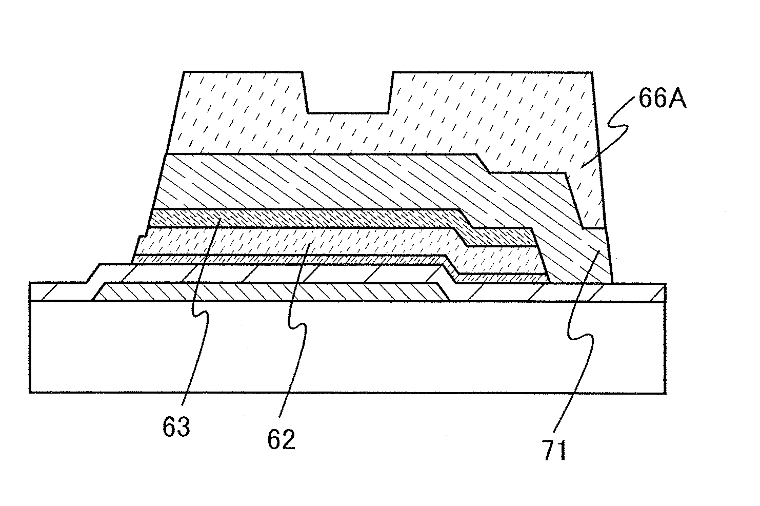
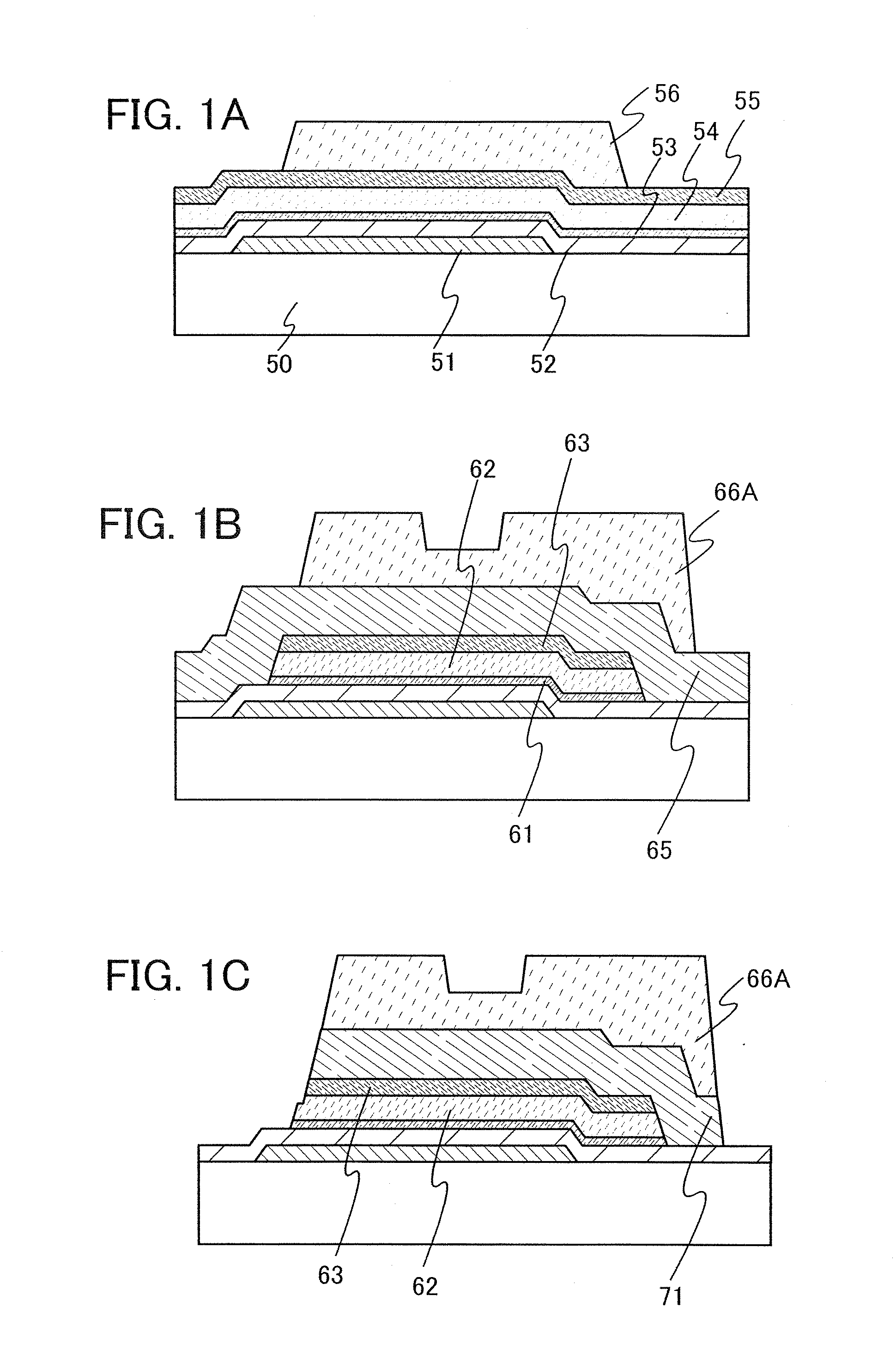
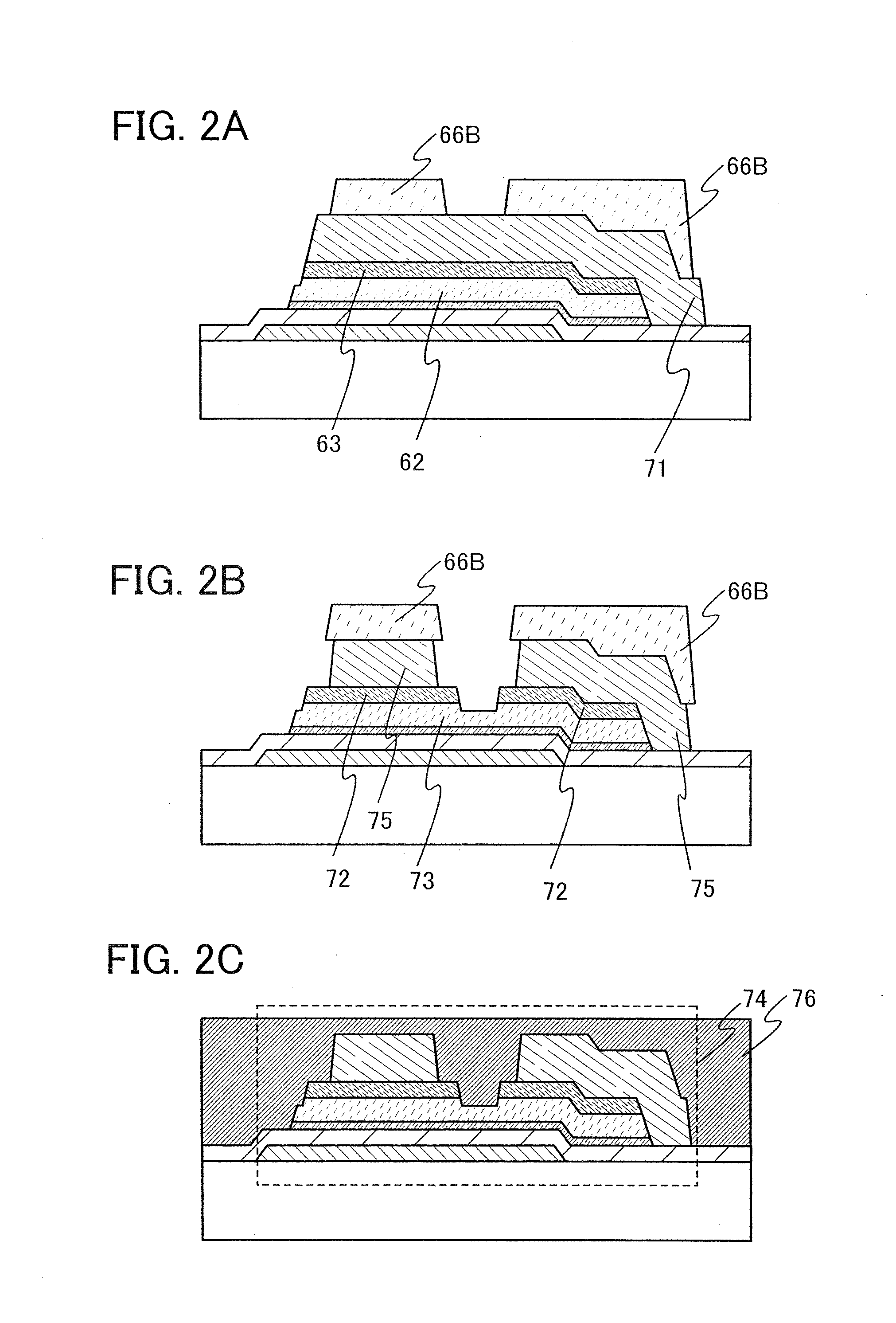
[0032]In this embodiment mode, a manufacturing process of an electrophoretic display device, in particular, a manufacturing process of a pixel having a thin film transistor are described with reference to FIGS. 1A to 1C, FIGS. 2A to 2C, FIGS. 3A and 3B, FIG. 4, FIGS. 5A and 5B, and FIGS. 6A to 6C. FIGS. 1A to 1C, FIGS. 2A to 2C, and FIGS. 3A and 3B are cross-sectional views illustrating a manufacturing process of a thin film transistor, FIG. 4 is a view for illustrating an electrophoretic display device, and FIGS. 5A and 5B are respectively a top view and a longitudinal sectional view of a connection region of a thin film transistor and a pixel electrode in a pixel. Further, FIGS. 6A to 6C illustrate appearances of an electrophoretic display device.

[0033]An n-channel thin film transistor having a microcrystalline semiconductor film is more suitable for use in a driver circuit than a p-channel thin film transistor having a microcrystalline semiconductor film because it has a higher m...

embodiment mode 2

[0092]In this embodiment mode, a manufacturing process, which is a different process of the electrophoretic display device shown in Embodiment Mode 1, is described with reference to FIGS. 7A to 7B and FIGS. 8A and 8B.

[0093]First, a molybdenum film 702 is formed over a supporting substrate 701. As the supporting substrate 701, a glass substrate, a ceramics substrate, or a quartz substrate can be used. In this embodiment mode, a glass substrate is used. The molybdenum film 702 is a molybdenum film formed by a sputtering method with a thickness of 30 to 200 nm. Since the substrate may be fixed in the sputtering method, the thickness of the molybdenum film in the vicinity of the edge portion of the substrate tends to be nonuniform. Therefore, the molybdenum film on the edge portion is preferably removed by dry etching.

[0094]Next, a molybdenum oxide film 703 is formed by oxidation of a surface of the molybdenum film 702. The molybdenum oxide film 703 may be formed by oxidation of the sur...

embodiment mode 3

[0108]In this embodiment, the appearance and the cross section of an electrophoretic display device of the present invention is described with reference to FIGS. 9A and 9B. FIGS. 9A and 9B are views of an electrophoretic display device in which a thin film transistor 4010 including a microcrystalline semiconductor film and an electrophoretic display element 4008 which are formed over a first flexible substrate 4001 are sealed with a sealant 4005 between the first substrate 4001 and a second flexible substrate 4006. FIG. 9B is a cross-sectional view taken along line A-A′ of FIG. 9A.

[0109]A sealant 4005 is provided so as to surround a pixel portion 4002 and a scan line driver circuit 4004 which are provided over the first flexible substrate 4001. Further, the second flexible substrate 4006 is provided over the pixel portion 4002 and the scan line driver circuit 4004. Therefore, the pixel portion 4002 and the scan line driver circuit 4004 as well as the electrophoretic display element ...


PUM


Abstract

It is an object to provide an electrophoretic display device having a thin film transistor which has highly reliable electric characteristics, lightweight, and flexibility. A gate insulating film is formed over a gate electrode, a microcrystalline semiconductor film which functions as a channel formation region is formed over the gate insulating film, a buffer layer is formed over the microcrystalline semiconductor film, a pair of source and drain regions are formed over the buffer layer, a pair of the source and drain electrodes in contact with the source and drain regions are formed. Then, the inverted-staggered thin film transistor is interposed between the flexible substrates, and the thin film transistor is provided with electrophoretic display element which is electrically connected by the pixel electrode. Then, the electrophoretic display electrode is surrounded by the partition layer so as to cover the end portion of the pixel electrode and provided over the pixel electrode.

Description

BACKGROUND OF THE INVENTION[0001]1. Field of the Invention[0002]The present invention relates to a display device and a method for manufacturing the display device provided with an electrophoretic display element for displaying images in such a manner that fine particles dispersed in a solvent is made to move or rotate according to voltage application to an interposed electrode so that the reflectivity is changed. The present invention relates to, in particular, an electrophoretic display device and the method for manufacturing the electrophoretic display device which is formed by combining an electrophoretic display element and a thin film transistor (hereinafter, referred to as a TFT) in which a channel region is formed using a microcrystalline semiconductor.[0003]2. Description of the Related Art[0004]In recent years, electronic paper (also referred to as digital paper or a paper like display) is attracted attention and some of it is put into practical use. The form that the elec...

Claims


Application Information

Patent Timeline
IPC IPC(8): H01L29/04H01L21/336G02F1/167G02F1/16755G02F1/16757G02F1/1679
CPCG02F1/1368G02F1/167H01L27/1214H01L27/1266H01L29/78696H01L29/78603H01L29/78669H01L29/78678H01L29/04H01L27/1218G02F1/1679G02F1/16757G02F1/16755
Inventor YAMAZAKI, SHUNPEI
Owner SEMICON ENERGY LAB CO LTD
Why Eureka
Try Eureka