Electron multiplication CMOS imager

a cmos imager and multi-core technology, applied in the field of imaging systems, can solve the problems of large size imagers that are expensive and increase the number, and achieve the effect of more amplification

Inactive Publication Date: 2009-04-02
SRI INTERNATIONAL
View PDF12 Cites 22 Cited by
  • Summary
  • Abstract
  • Description
  • Claims
  • Application Information

AI Technical Summary

Problems solved by technology

Unfortunately for the Burt et al. design, the increasing demand from the consumer market to supply higher and higher resolution CCD cameras has required designers to increase the number of pixels in the CCD image sensors that are used in these products.
The separate imaging area and storage area in the Burt et al. design goes against this trend, resulting in a large size imager that is costly.

Method used


Image

  • Electron multiplication CMOS imager
  • Electron multiplication CMOS imager
  • Electron multiplication CMOS imager

Examples


Embodiment Construction

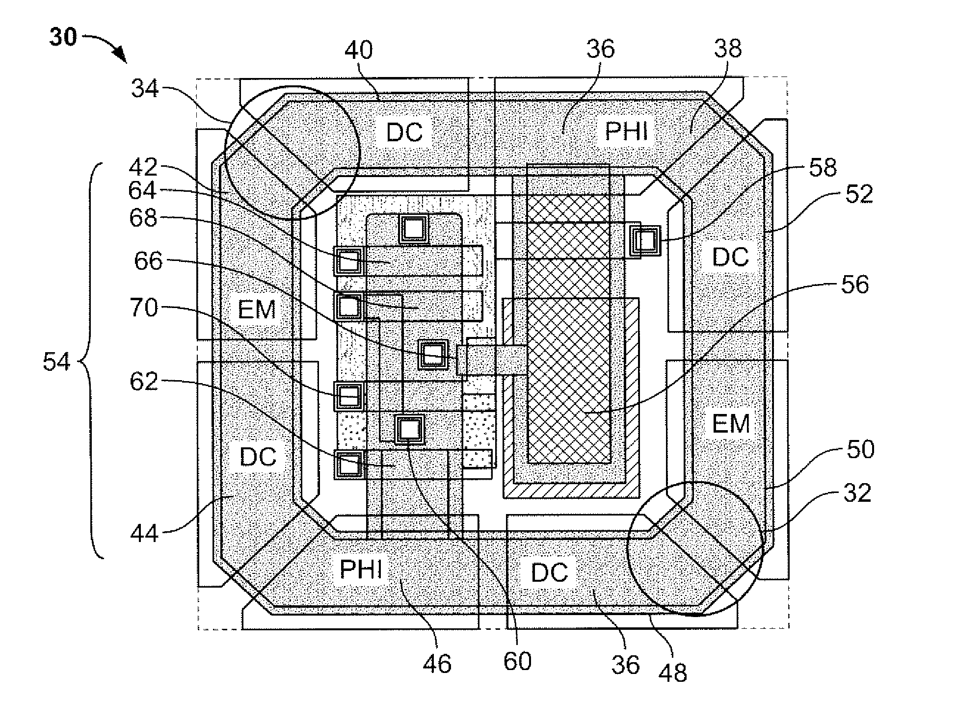
[0023]Referring now to FIGS. 3A and 3B, plan views of an EMCMOS device layout and architecture is depicted. Rather than having separate charge collection, storage, and electron multiplication (EM) regions, all three functions are incorporated into a single pixel 30 formed monolithically as an integrated circuit. The pixel 30 includes one or more electron multiplication (EM) gain regions 32, 34 whose accumulated charge circulates around an enclosed track or circulating register called the EM gain register 36. In FIGS. 3A, 3B, there are a total of eight gates which constitute two stages of the EM gain register 36: PHI (clocked gate) 38, DC gate 40, EM (high voltage clocked gate) 42, DC gate 44, PHI 46, DC Gate 48, EM 50, and DC Gate 52. A readout structure 54 comprising a number of sub-structures are fabricated in the pixel 30 nested within the EM gain register 36. The light sensitive area, which creates electrons in proportion to the radiant energy incident on the pixel 30 can be an ...


PUM


Abstract

A pixel for an imager is disclosed that includes at least one electron multiplication (EM) gain stage configured in a loop and electrically coupled to a charge collection region and a charge readout region, the charge collection region being configured to generate a charge packet, the EM gain stage being configured to amplify the charge packet by impact ionization and to circulate the charge packet a predetermined number of times in one direction around the loop, the charge readout region being configured to receive the amplified charge packet and convert the amplified charge to a measurable signal. The at least one EM gain stage, the charge collection region, and the charge readout region can be formed monolithically in an integrated circuit. The pixel can be manufactured using a CMOS process. The pixel can further include a second EM gain stage formed in the integrated circuit to increase the amount of amplification around the loop.

Description

FIELD OF THE INVENTION[0001]The present invention relates generally to imaging systems, and more particularly to the design of a CMOS-based imaging pixel which employs a form of electron multiplication (impact ionization) gain.BACKGROUND OF THE INVENTION[0002]A ubiquitous image sensor technology used in digital cameras is the charge-coupled device (CCD) imager. In a typical CCD imager, signal charge representative of incident radiation is accumulated in an array of pixels in an image area. Following an integration period, the signal charge is transferred to an output register by applying appropriate clocking or drive pulses to control electrodes. The signal charge is then read out from the output register and applied to a charge detection circuit to produce a voltage, which is representative of the amount of signal charge.[0003]It has been found that, with the application of proper gate potentials, a form of gain via impact ionization can be achieved in a CCD device. In a thesis ent...

Claims


Application Information

Patent Timeline
Patent Type & Authority Applications(United States)
IPC IPC(8): H04N5/235H04N5/335
CPCH01L27/14609H04N5/37452H04N5/335H01L27/14837H04N25/00H04N25/771
Inventor TOWER, JOHN ROBERTSONANDREWS, JAMES TYNAN
Owner SRI INTERNATIONAL
Why Eureka
Try Eureka