Capacitors Integrated with Metal Gate Formation

a technology of metal oxide metal and capacitors, applied in the direction of capacitors, diodes, semiconductor/solid-state device details, etc., can solve the problems of limited inability to increase k value, and inability to reduce thickness and k value, so as to improve electrical performance and improve electrical performance without increasing manufacturing costs

Active Publication Date: 2009-04-09
TAIWAN SEMICON MFG CO LTD
View PDF23 Cites 58 Cited by
  • Summary
  • Abstract
  • Description
  • Claims
  • Application Information

AI Technical Summary

Benefits of technology

[0015]The advantageous features of the present invention include forming capacitors with increased capacitance and improved electrical performance without increasing the manufacturing cost.

Problems solved by technology

However, the thickness and the k value are often limited by the technology used for forming the capacitor.
For example, the thickness cannot be less than what the existing technology allows.
On the other hand, since the capacitors are often formed in low-k dielectric layers, the ability to increase the k value is also limited.
A problem associated with increasing area is that greater chip area is required.
However, the use of polysilicon causes the degradation of the high-frequency response of the MOM capacitors, particularly at frequencies of about 1 GHz or higher.

Method used


Image

  • Capacitors Integrated with Metal Gate Formation
  • Capacitors Integrated with Metal Gate Formation
  • Capacitors Integrated with Metal Gate Formation

Examples


Embodiment Construction

[0025]The making and using of the presently preferred embodiments are discussed in detail below. It should be appreciated, however, that the present invention provides many applicable inventive concepts that can be embodied in a wide variety of specific contexts. The specific embodiments discussed are merely illustrative of specific ways to make and use the invention, and do not limit the scope of the invention.

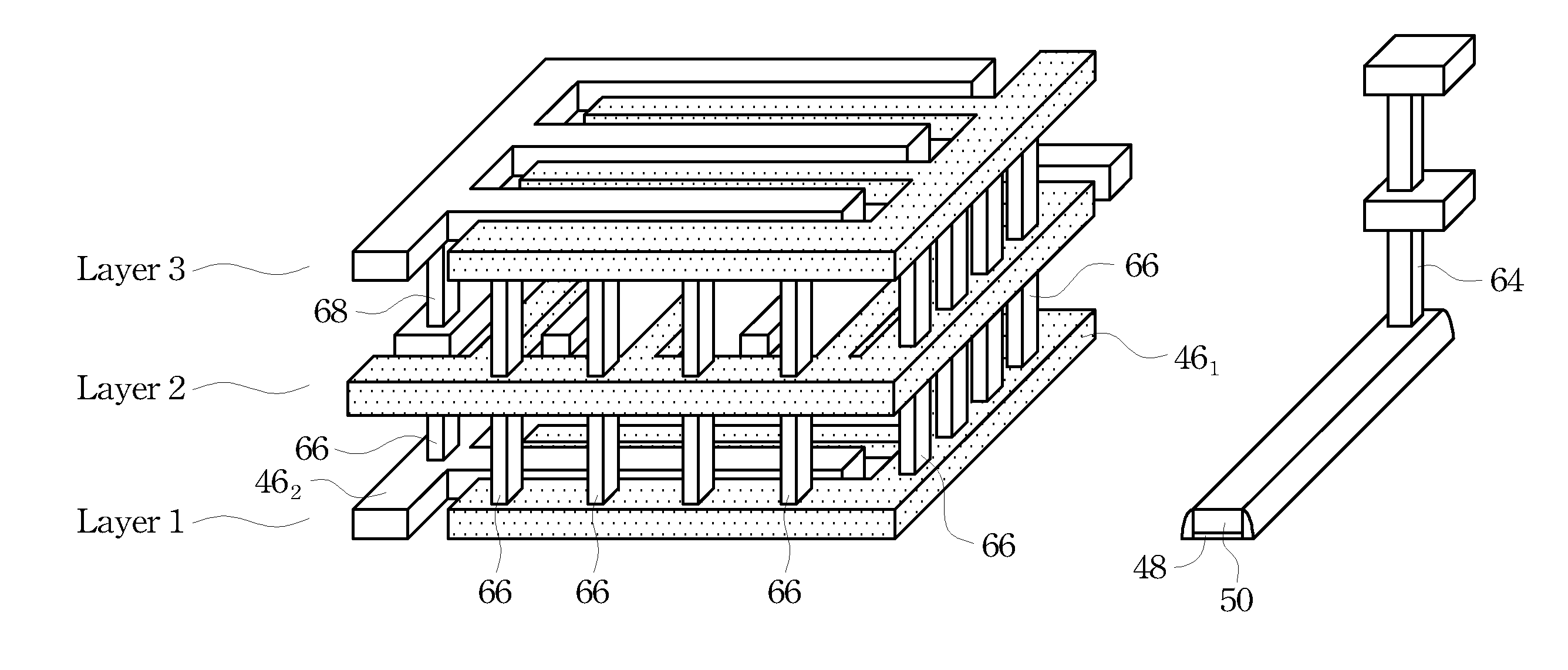
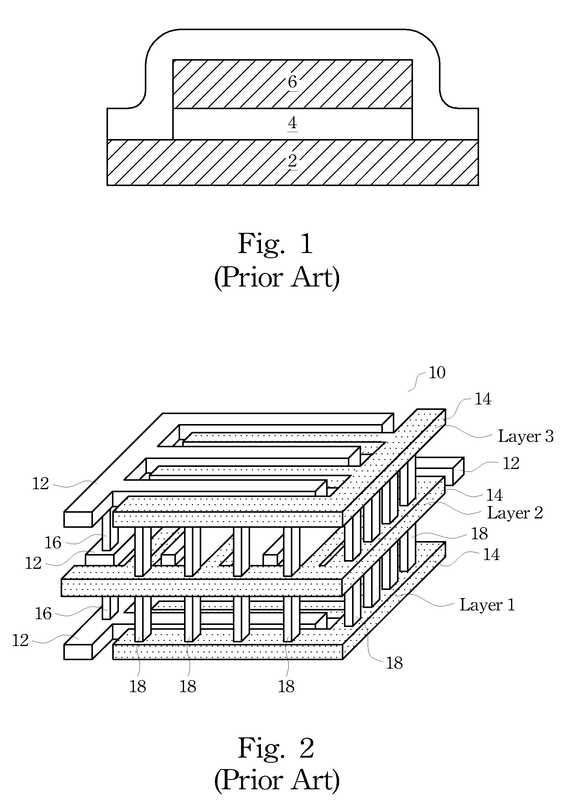
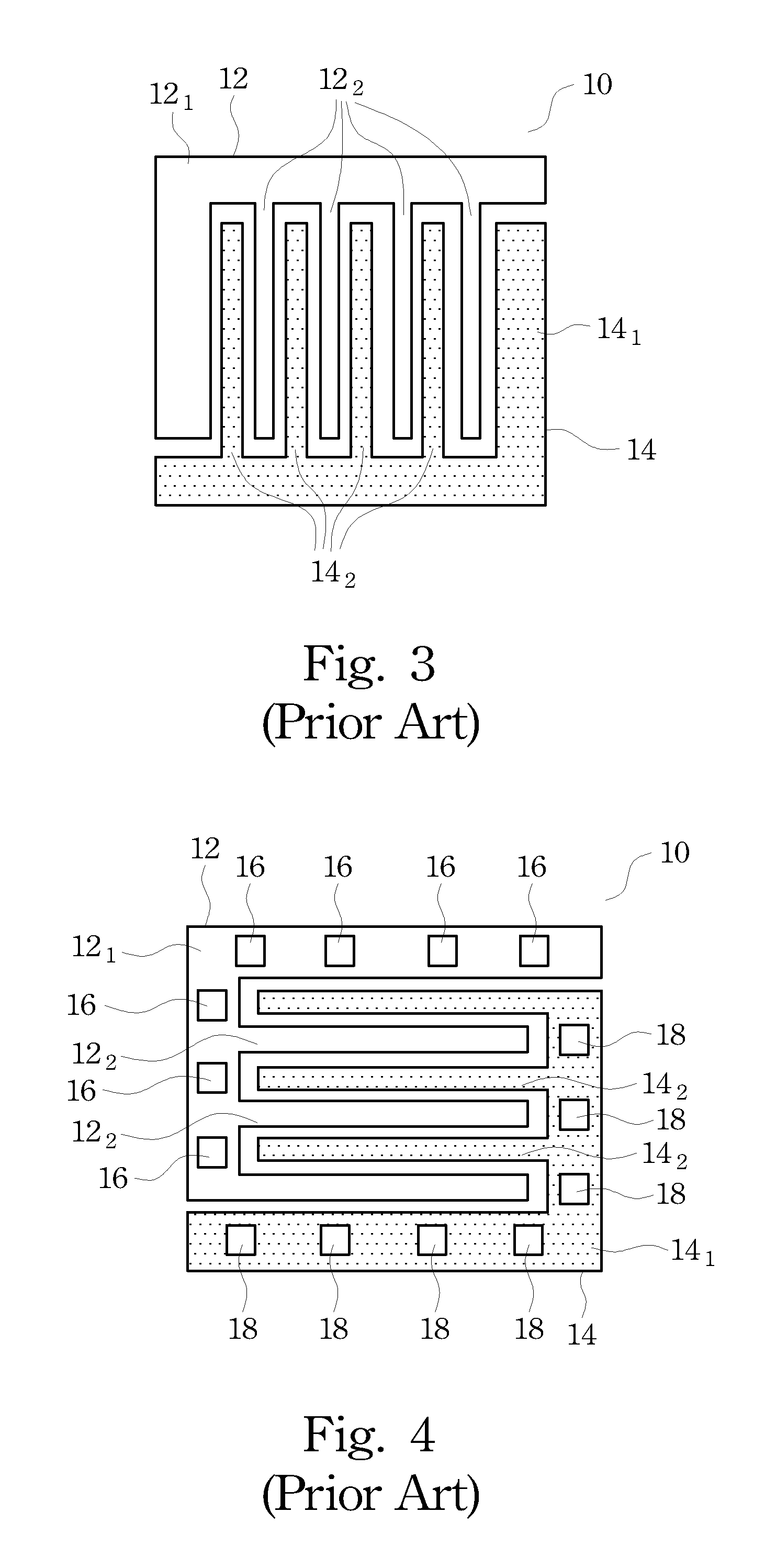
[0026]Metal-oxide-metal (MOM) and metal-insulator-metal (MIM) capacitor structures and the methods of forming the same are provided. The intermediate stages of manufacturing the preferred embodiments of the present invention are illustrated. The variations of the preferred embodiments are then discussed. Throughout the various views and illustrative embodiments of the present invention, like reference numbers are used to designate like elements.

[0027]Referring to FIG. 5, substrate 30 is provided. Substrate 30 may include a semiconductor material such as silicon, silicon germa...


PUM


Abstract

A semiconductor structure including a capacitor having increased capacitance and improved electrical performance is provided. The semiconductor structure includes a substrate; and a capacitor over the substrate. The capacitor includes a first layer including a first capacitor electrode and a second capacitor electrode, wherein the first capacitor electrode is formed of a metal-containing material and is free from polysilicon. The semiconductor structure further includes a MOS device including a gate dielectric over the substrate; and a metal-containing gate electrode on the gate dielectric, wherein the metal-containing gate electrode is formed of a same material, and has a same thickness, as the first capacitor electrode.

Description

TECHNICAL FIELD[0001]This invention relates generally to semiconductor devices, and more particularly to layout design and manufacturing methods of metal-oxide-metal capacitors.BACKGROUND[0002]Metal-insulator-metal (MIM) capacitors and metal-oxide-metal (MOM) capacitors are among the most widely used capacitors in integrated circuits. FIG. 1 illustrates a typical MIM capacitor, which includes bottom plate 2, top plate 6, and insulation layer 4 therebetween. The bottom plate 2 and top plate 6 are formed of conductive materials.[0003]As is known in the art, the capacitance of a capacitor is proportional to its area and the dielectric constant (k) of the insulation layer, and is inversely proportional to the thickness of the insulation layer. Therefore, to increase the capacitance, it is preferable to increase the area and the k value and to reduce the thickness of the insulation layer. However, the thickness and the k value are often limited by the technology used for forming the capa...

Claims


Application Information

Patent Timeline
Patent Type & Authority Applications(United States)
IPC IPC(8): H01L27/108
CPCH01L23/5223H01L27/0629H01L28/60H01L27/11568H01L27/105H01L2924/0002H10B43/30H01L2924/00
Inventor CHANG, CHUNG-LONGLU, DAVID DING-CHUNGCHEN, CHIA-YIWU, I-LU
Owner TAIWAN SEMICON MFG CO LTD
Why Eureka
Try Eureka