Multi-resolution Image Sensor Array with High Image Quality Pixel Readout Circuitry

a readout circuit technology, applied in the field of electronic imaging devices, can solve the problems of low manufacturing yield and high cost, use of cmos aps technology, and low manufacturing yield, and achieve high-performance multi-resolution image sensor arrays. , the effect of improving the performan

Inactive Publication Date: 2009-04-09
CMOS SENSOR
View PDF9 Cites 68 Cited by
  • Summary
  • Abstract
  • Description
  • Claims
  • Application Information

AI Technical Summary

Benefits of technology

[0009]The present invention discloses a configurable multi-resolution linear image sensor array using only two thirds, i.e., around 2000, of the number of PE used in the first aforementioned prior art predating the U.S. Pat. No. 5,949,483. Yet the present invention does not require as much extra circuitry as the one disclosed in the U.S. Pat. No. 5,949,483 except for adding only one transistor switch between a PE and the input of the readout circuit in an APS thus keeping the cost of the imager low while improving its performance. The present invention amounts to an improved high performance multi-resolution image sensor array using a small number of photo-detector elements and minimal readout circuitry for achieving the multiple resolutions. Furthermore, comparing with the aforementioned prior arts for implementing an APS, the present invention further provides an in-pixel correlated multiple sampling (CMS) circuitry for converting an input photoelectric signal, generated by a switch-resettable photoelectric conversion amplifier in response to an incoming image light pixel, into a corresponding output video signal. The improved APS circuitry thus achieves higher image quality by accommodating snapshot image capture operation while minimizing the FPN and the kTCN with minimal additional circuitry.

Problems solved by technology

Hence, such prior art arrays consume relatively large device area with a large number of photo-detector elements (PE) results in relatively low manufacturing yield and high cost.
As a result, this approach is still relatively expensive.
However, as of today the major drawbacks of using CMOS APS technology still include significant reset kTC noise (kTCN), significant fixed pattern noise (FPN) and image lag accompanying an array of a large number of PE.
Their disadvantages include FPN originated from the so-called source follower used in the circuit and reset noise, i.e. kTCN, originated from resetting the CMOS APS circuitry of the photo-detector array.
The advantages include lower FPN and good linearity but the disadvantages include the presence of reset kTCN.
The advantages include low FPN, good linearity and controllable gain with disadvantages including the reset kTCN plus it is not suitable for snapshot image capture operation.
While the CDS circuitry reduces the reset kTCN, it requires dedicated memory elements either on or off a CMOS chip hence resulting in higher cost.
As the reset kTCN is correlated following a single reset pulse but uncorrelated between separate reset pulses, the prior art CDS circuitry does not effectively minimize the kTCN.

Method used


Image

  • Multi-resolution Image Sensor Array with High Image Quality Pixel Readout Circuitry
  • Multi-resolution Image Sensor Array with High Image Quality Pixel Readout Circuitry
  • Multi-resolution Image Sensor Array with High Image Quality Pixel Readout Circuitry

Examples


Embodiment Construction

[0023]The description above and below plus the drawings contained herein merely focus on one or more currently preferred embodiments of the present invention and also describe some exemplary optional features and / or alternative embodiments. The description and drawings are presented for the purpose of illustration and, as such, are not limitations of the present invention. Thus, those of ordinary skill in the art would readily recognize variations, modifications, and alternatives. Such variations, modifications and alternatives should be understood to be also within the scope of the present invention.

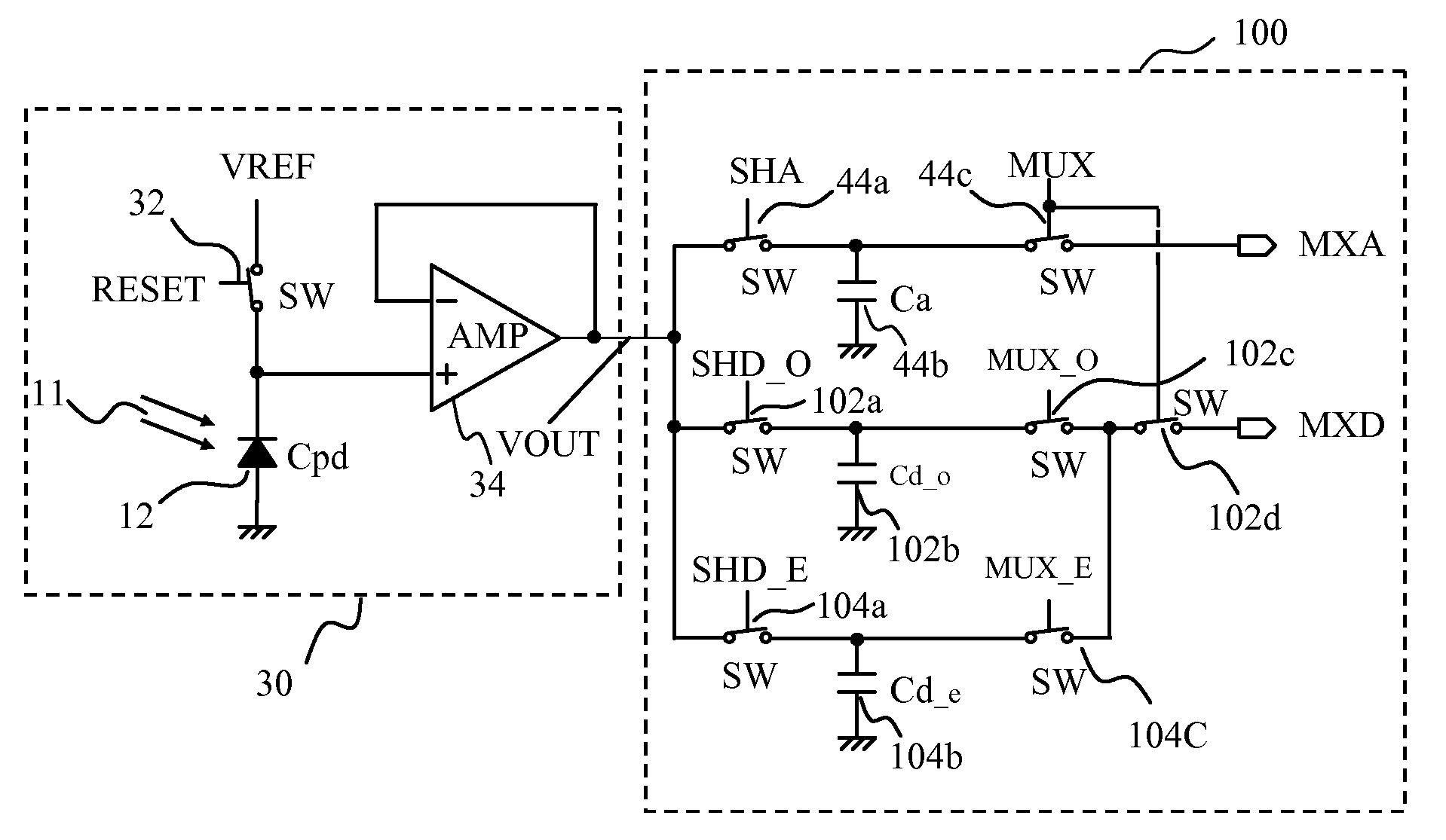
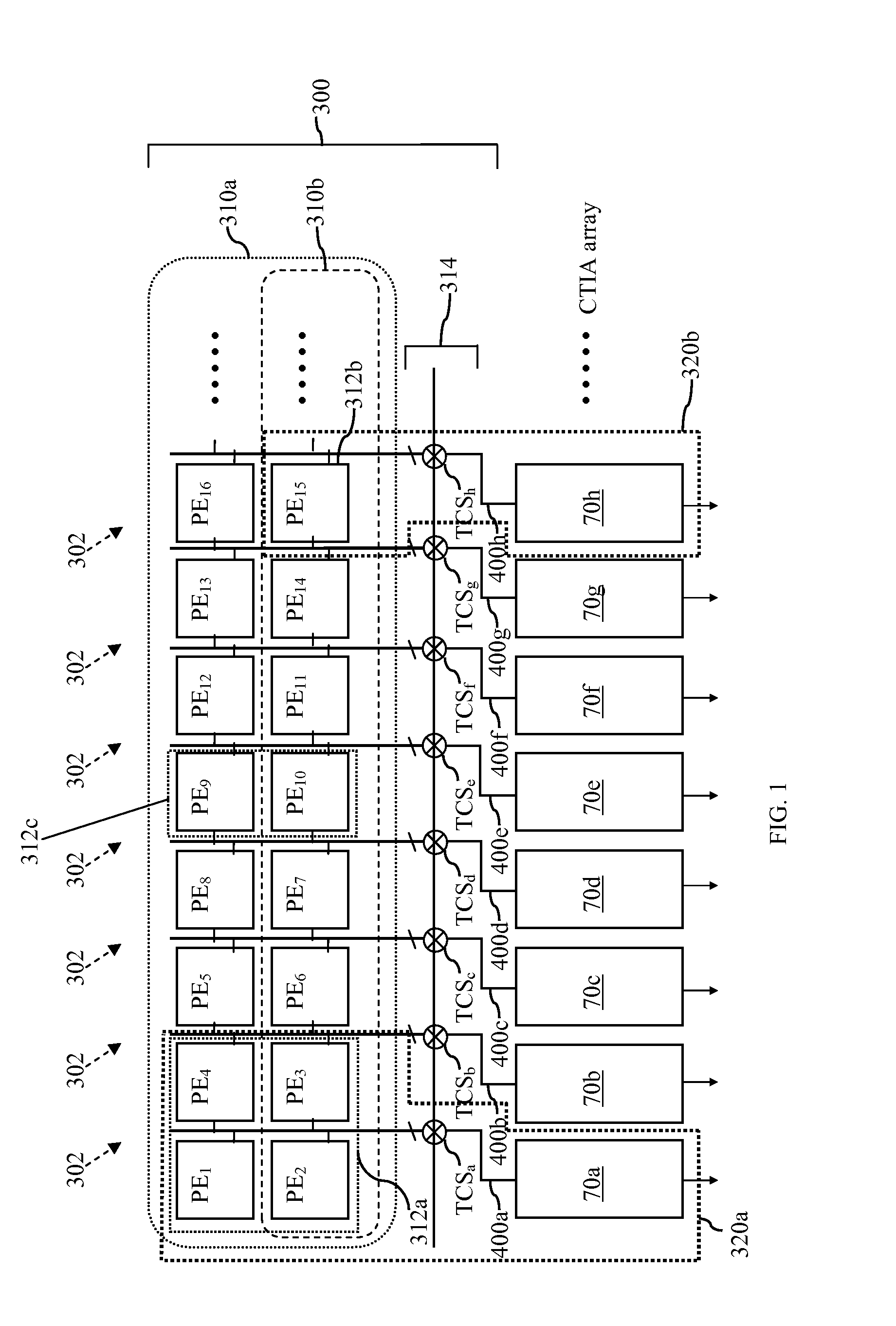
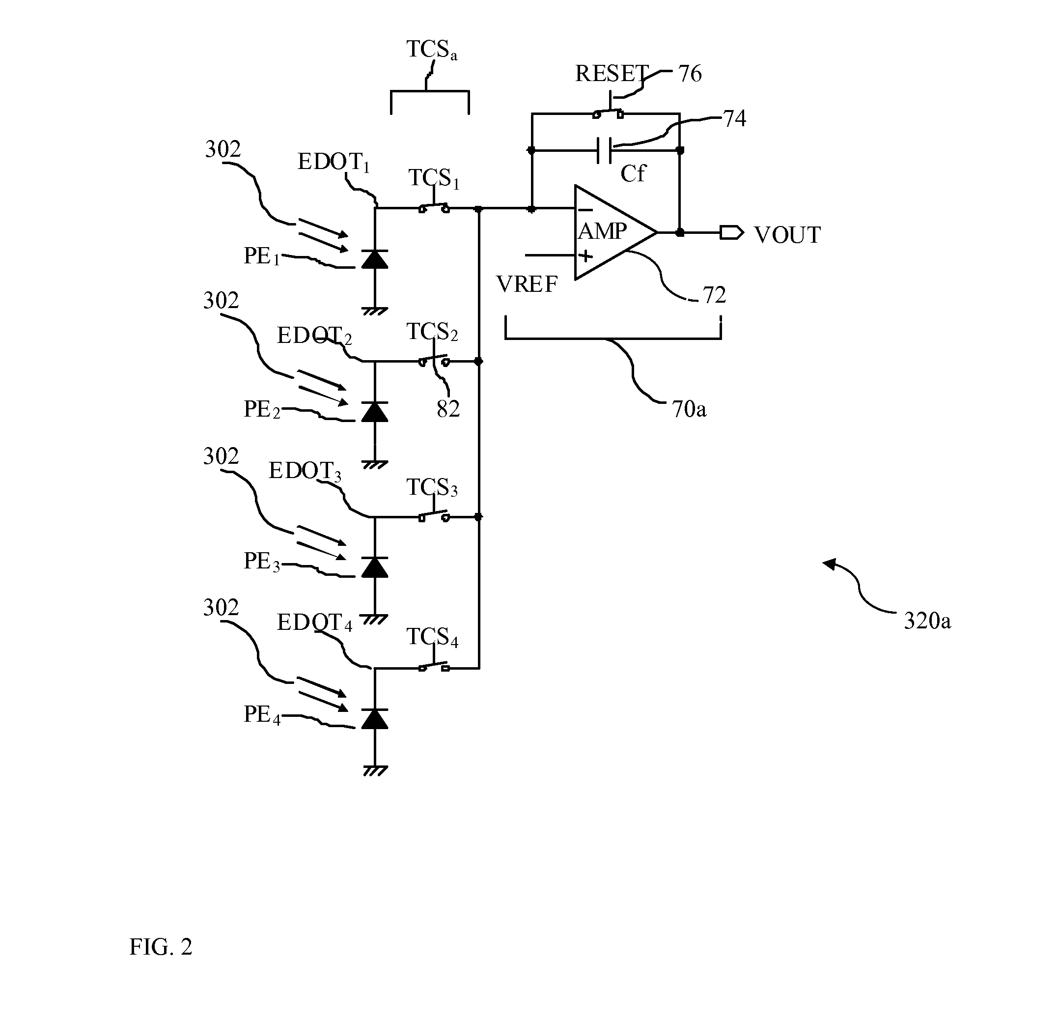
[0024]FIG. 1 is a simplified schematic block diagram illustrating the architecture of a preferred embodiment of a multi-resolution image sensor array 300 of the present invention for converting an incoming image light 302 into a corresponding array of image signals 400a, 400b, 400c, 400d, 400e, etc. The multi-resolution image sensor array 300 has a number of photo-detector elements PE1,...


PUM


Abstract

A configurable, compact multi-resolution linear image sensor array is disclosed. The multi-resolution image sensor array employs a spatial array of photoelectric sites with each site having an image output terminal and a cluster of switched photo-detector elements. To effect a high quality snapshot operation mode for a high pixel count array, a transfer control switch is added bridging each photo-detector element and its correspondingly connected negative input terminal of an operational amplifier to form an active pixel sensor circuit. To minimize a reset kTC noise associated with numerous traditional active pixel sensor circuits, an in-pixel KTC noise-correlated correlated multiple sampling (CMS) circuitry is also proposed to replace an otherwise traditional correlated double sampling (CDS) circuitry.

Description

BACKGROUND OF THE INVENTION[0001]1. Field of the Invention[0002]The present invention relates to electronic imaging devices. More specifically, the invention provides an apparatus of configurable resolutions using a small number of photo-detector elements (PE) to form a compact multi-resolution sensor array and for reducing signal noises in an MOS active pixel sensor (APS) circuitry.[0003]2. Description of Related Arts[0004]A multi-resolution linear image sensor array from a prior art typically includes dedicated and separated arrays of photoelectric sensing elements each corresponding to a particular resolution. Hence, such prior art arrays consume relatively large device area with a large number of photo-detector elements (PE) results in relatively low manufacturing yield and high cost. For example, a dual-resolution, 300 dots-per-inch (dpi) and 600 dots-per-inch (dpi), image sensor array includes two dedicated arrays of PE for the two resolutions using 2000 image sensing elements...

Claims


Application Information

Patent Timeline
Patent Type & Authority Applications(United States)
IPC IPC(8): H04N5/335H04N5/363H04N5/365H04N5/374H04N5/378
CPCH04N5/335H04N5/378H04N5/357H04N5/347H04N25/00H04N25/46H04N25/60H04N25/75
Inventor LIN, SHENGMINWANG, WENG-LYANG
Owner CMOS SENSOR
Why Eureka
Try Eureka