Organic electro-luminescent display device

a display device and electroluminescent technology, applied in the manufacture of electrode systems, electric discharge tubes/lamps, discharge tubes luminescnet screens, etc., can solve the problems of affecting the quality of light, so as to enhance the reliability of light, prevent the occurrence of conduction failure, and improve the effect of brightness

Active Publication Date: 2009-04-16
SAMSUNG DISPLAY CO LTD +1
View PDF3 Cites 30 Cited by
  • Summary
  • Abstract
  • Description
  • Claims
  • Application Information

AI Technical Summary

Benefits of technology

[0026]According to the present invention, the auxiliary electrodes are formed by mask vapor deposition or mask sputtering and hence, the formation of the auxiliary electrodes requires no photolithography step thus realizing the formation of the auxiliary electrodes without largely pushing up a manufacturing cost.
[0027]Further, although the connection between a current supply line which supplies an electric current to the upper electrode and the auxiliary electrode is established via the through hole formed in the insulation film, the through hole is extremely deep in general and hence, the conduction failure is liable to occur. According to the present invention, in place of establishing the connection with the current supply line using only the auxiliary electrode formed on the through hole, the contact electrode is formed in an overlapping manner with the auxiliary electrode at the through hole and hence, it is possible to prevent the occurrence of conduction failure at the contact portion.
[0028]In this manner, according to the present invention, it is possible to suppress a phenomenon that a potential of the upper electrode differs depending on a place and, at the same time, it is possible to enhance reliability of conduction between the current supply line and the upper electrode. Accordingly, it is possible to provide a top-emission-type organic EL display device which exhibits excellent uniformity of brightness and high reliability.

Problems solved by technology

Patterning of the auxiliary lines is performed by photolithography and hence, a manufacturing cost is pushed up.
The through hole formed in the bank is deep and hence, it is difficult to acquire the reliable conduction at the through hole portion.
Patterning of the auxiliary electrodes is performed by photolithography and hence, a manufacturing cost is pushed up.
Further, in the above-mentioned technique disclosed in patent document 2, although the bank is not formed between the pixels and the pixels, when the bank is formed, in the same manner as patent document 1, a drawback on the conduction at the through hole arises.

Method used


Image

  • Organic electro-luminescent display device
  • Organic electro-luminescent display device
  • Organic electro-luminescent display device

Examples


embodiment 1

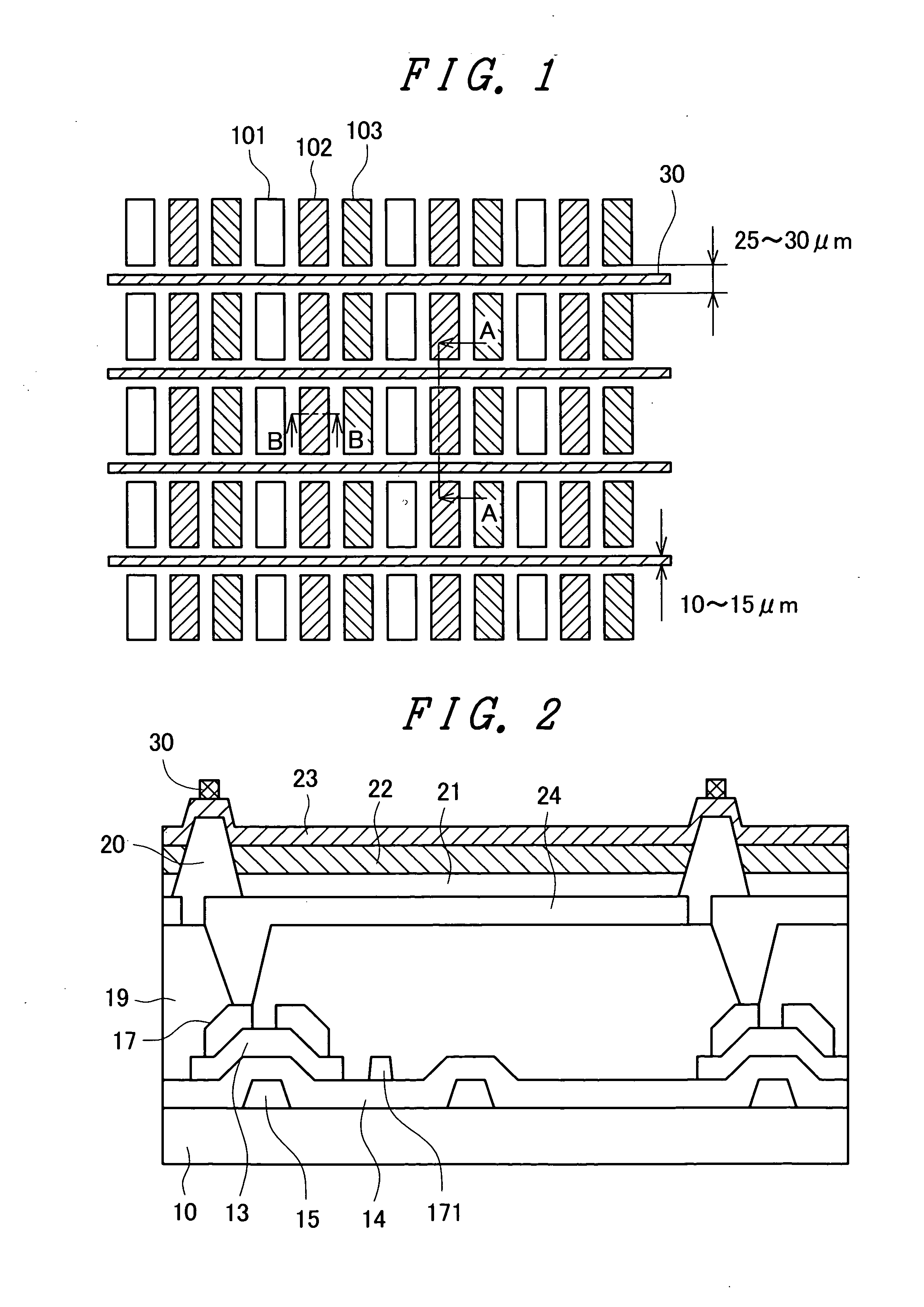
[0039]FIG. 1 is a plan view of a display region of a top-emission-type organic EL display device according to the present invention. FIG. 2 is across-sectional view taken along a line A-A in FIG. 1. In FIG. 1, a red pixel 101, a green pixel 102 and a blue pixel 103 are arranged sequentially in the lateral direction. The pixels having the same color are arranged in the longitudinal direction. Each pixel includes an organic EL layer 22 which emits color of red, green or blue. Each organic EL layer 22 is covered with an IZO film which constitutes a transparent electrode forming an upper electrode 23. The transparent electrode may be also formed of an ITO film or the like besides the IZO film.

[0040]An auxiliary electrode 30 extends in the lateral direction between the pixels and the pixels arranged in the longitudinal direction. The auxiliary electrode 30 is formed on the upper electrode 23 formed in a matted manner by mask vapor deposition. In the present invention, the auxiliary elect...

embodiment 2

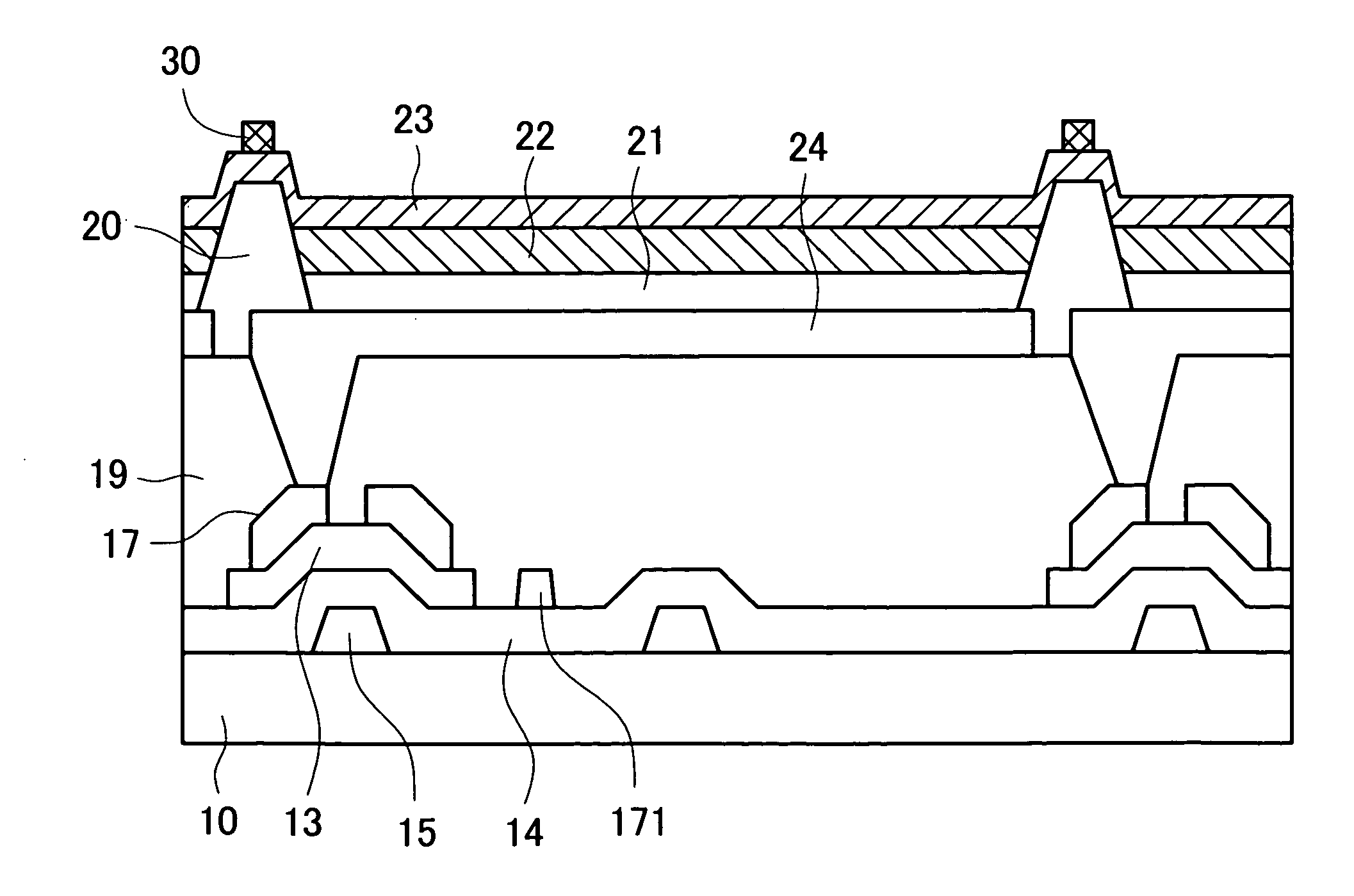
[0061]The present invention is, so long as the organic EL display device is the top-emission-type organic EL display device, applicable to irrespective of whether the organic EL layer 22 is of a top anode type or of a top cathode type and irrespective of whether the TFT is of a bottom gate type or of a top gate type. This embodiment is an example in which the present invention is applied to the case where the TFT is of a top gate type and the organic EL layer 22 is of a top anode type. FIG. 6 is a cross-sectional view of a pixel portion of this embodiment. FIG. 6 corresponds to a cross-sectional view taken along a line B-B in FIG. 1.

[0062]In FIG. 6, a first background film 11 made of SiN and a second background film 12 made of SiO2 are formed on an element substrate 10. These background films 11, 12 are provided for preventing impurities from a glass substrate from contaminating a semiconductor layer 13. The semiconductor layer 13 is formed on the second back ground film 12. With re...

embodiment 3

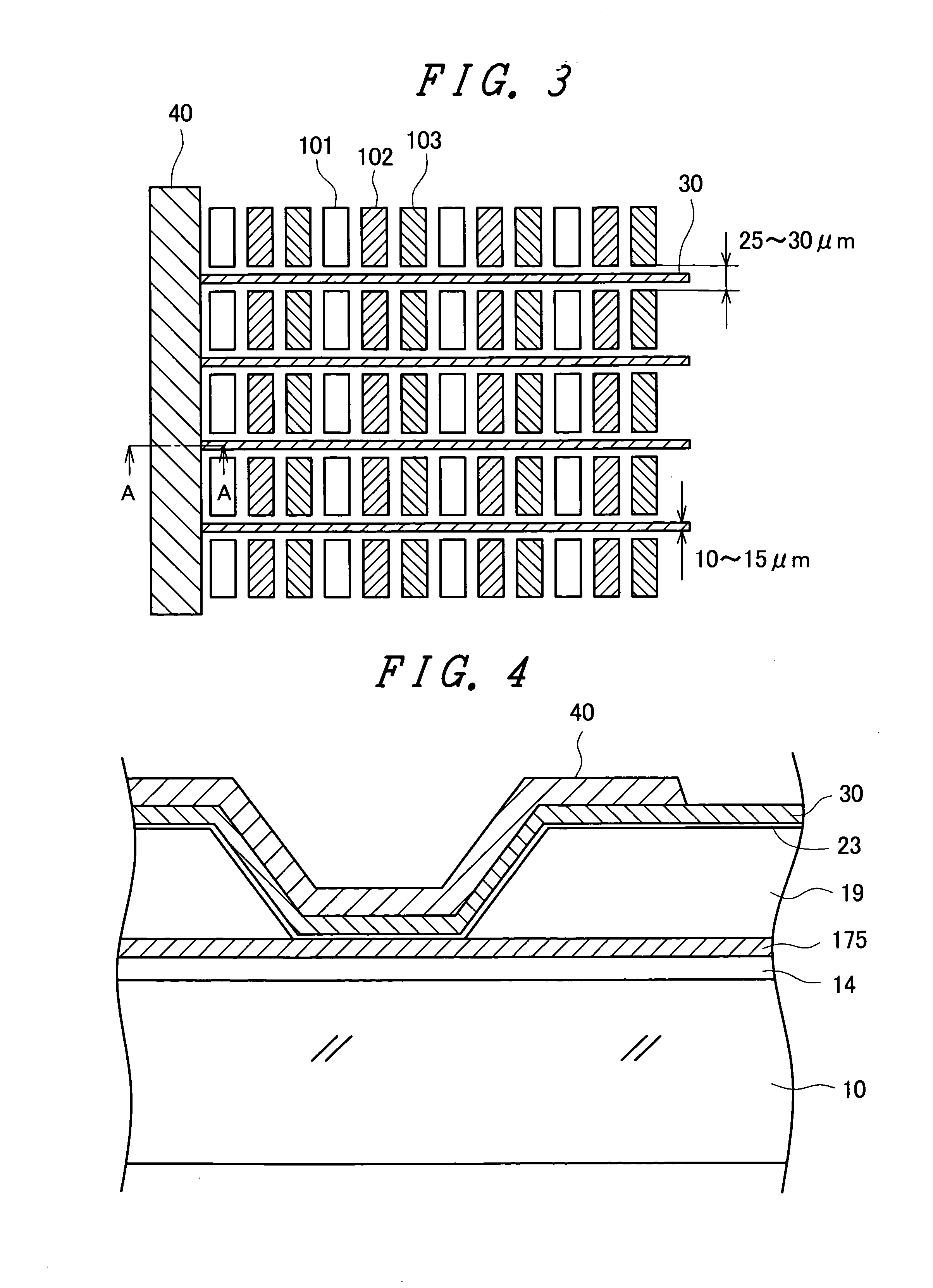
[0074]In the embodiment 1 and the embodiment 2, the supply of the electric current to the auxiliary electrodes 30 is collectively performed by providing a bus-like contact electrode 40 outside the display region in the lateral direction. The present invention is not limited to such cases, and is also applicable to a case in which the current supply line 175 and the auxiliary electrodes 30 are connected with each other within the display region. FIG. 8 is a plan view of the display region of this embodiment.

[0075]In FIG. 8, the pixels are arranged in the same manner as the pixels shown in FIG. 1. Further, the auxiliary electrodes 30 extend in the lateral direction on the screen in the same manner as the auxiliary electrodes 30 shown in FIG. 1. The embodiment 3 shown in FIG. 8 differs form the embodiment 1 shown in FIG. 1 with respect to a point that the contact of the auxiliary electrodes 30 and the current supply line is arranged within the display region. In FIG. 8, the contact por...


PUM


Abstract

A top-emission-type organic EL display device which exhibits uniform screen brightness is realized by preventing a voltage drop of an upper electrode formed of a transparent conductive film. Pixels each of which is sandwiched between an upper electrode and a lower electrode are arranged in a matrix array to form a display region. An auxiliary electrode extends in the lateral direction between the pixels and the pixels for preventing a voltage drop of the upper electrode. A current supply line which supplies an electric current to the upper electrode and the auxiliary electrodes are made conductive with each other by forming a through hole in an insulation layer. To ensure reliability of connection at the through hole, a contact electrode made of metal which overlaps with the auxiliary electrode is formed on the through hole by vapor deposition.

Description

CLAIM OF PRIORITY[0001]The present application claims priority from Japanese Application JP 2007-264503 filed on Oct. 10, 2007, the content of which is hereby incorporated by reference into this application.BACKGROUND OF THE INVENTION[0002]1. Field of the Invention[0003]The present invention relates to an organic electro-luminescent (EL) display device, and more particularly to a top-emission-type organic EL display device which can enhance the uniformity of brightness and can enhance the reliability of the organic EL display device.[0004]2. Description of the Related Art[0005]An organic EL display device is classified into a bottom-emission-type organic EL display device in which light emitted from organic EL layers is taken out in the direction of a glass substrate on which the organic EL layers and the like are formed and a top-emission-type organic EL display device in which light emitted from organic EL layers is taken out in the direction opposite to a glass substrate on which...

Claims


Application Information

Patent Timeline
Patent Type & Authority Applications(United States)
IPC IPC(8): H01J1/30H01J9/227
CPCH01L2251/5315H01L27/3276H10K59/131H10K2102/3026
Inventor MATSUDATE, NORIHARUOOKAWARA, TAKESHI
Owner SAMSUNG DISPLAY CO LTD
Why Eureka
Try Eureka