Method of Forming Vias in Silicon Carbide and Resulting Devices and Circuits

Inactive Publication Date: 2009-04-23
WOLFSPEED INC
View PDF39 Cites 260 Cited by
  • Summary
  • Abstract
  • Description
  • Claims
  • Application Information

AI Technical Summary

Benefits of technology

[0040]The invention meets this object with a method of etching a via through a semiconductor device formed in epitaxial layers on a silicon carbide substrate that has first and second surfaces on opposite sides of the substrate. The epitaxial layers comprise Group III nitride semiconductor material on the second surface of the silicon carbide substrate with respective platinum contacts defining the source, gate, and drain regions of the device therein. The invention comprises a method of etching a via through the silicon carbide substrate with a first etchant that removes the sil

Problems solved by technology

For example, although discrete (i.e., individual) silicon (Si) based devices can operate at microwave frequencies, silicon-based integrated circuits suffer from lower electron mobility and are generally disfavored for frequencies above about 3-4 GHz.
Silicon's inherent conductivity also limits the gain that can be delivered at high frequencies.
Although wire bonding techniques can be used for other devices that operate at other frequencies, they are disadvantageous at microwave frequencies in silicon carbide devices.
In particular, wires tend to cause undesired inductance at the microwave frequencies at which silicon carbide devices are capable of operating.
To date, however, opening vias in silicon carbide has been rather difficult because of its extremely robust physical characteristics, which, as noted above, are generally advantageous for most other purposes.
Silicon carbide does not lend itself rapidly to wet etching because of SiC's stability and

Method used


Image

  • Method of Forming Vias in Silicon Carbide and Resulting Devices and Circuits
  • Method of Forming Vias in Silicon Carbide and Resulting Devices and Circuits
  • Method of Forming Vias in Silicon Carbide and Resulting Devices and Circuits

Examples


Embodiment Construction

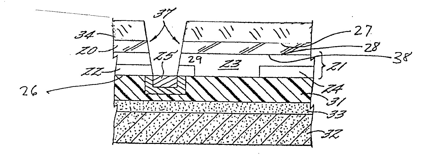
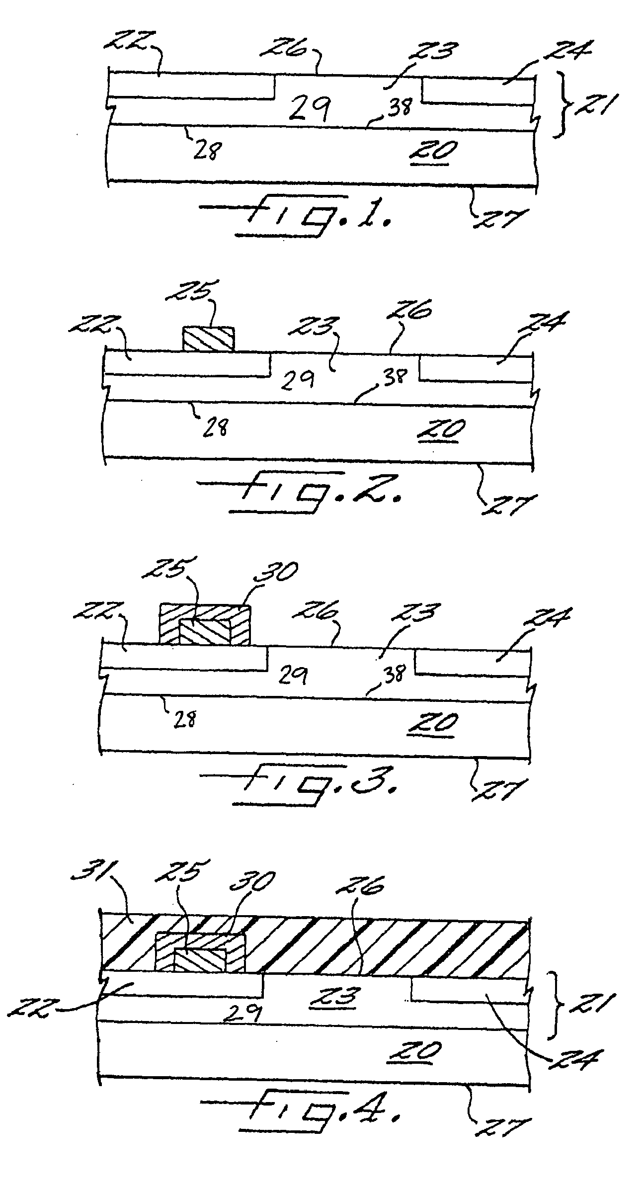
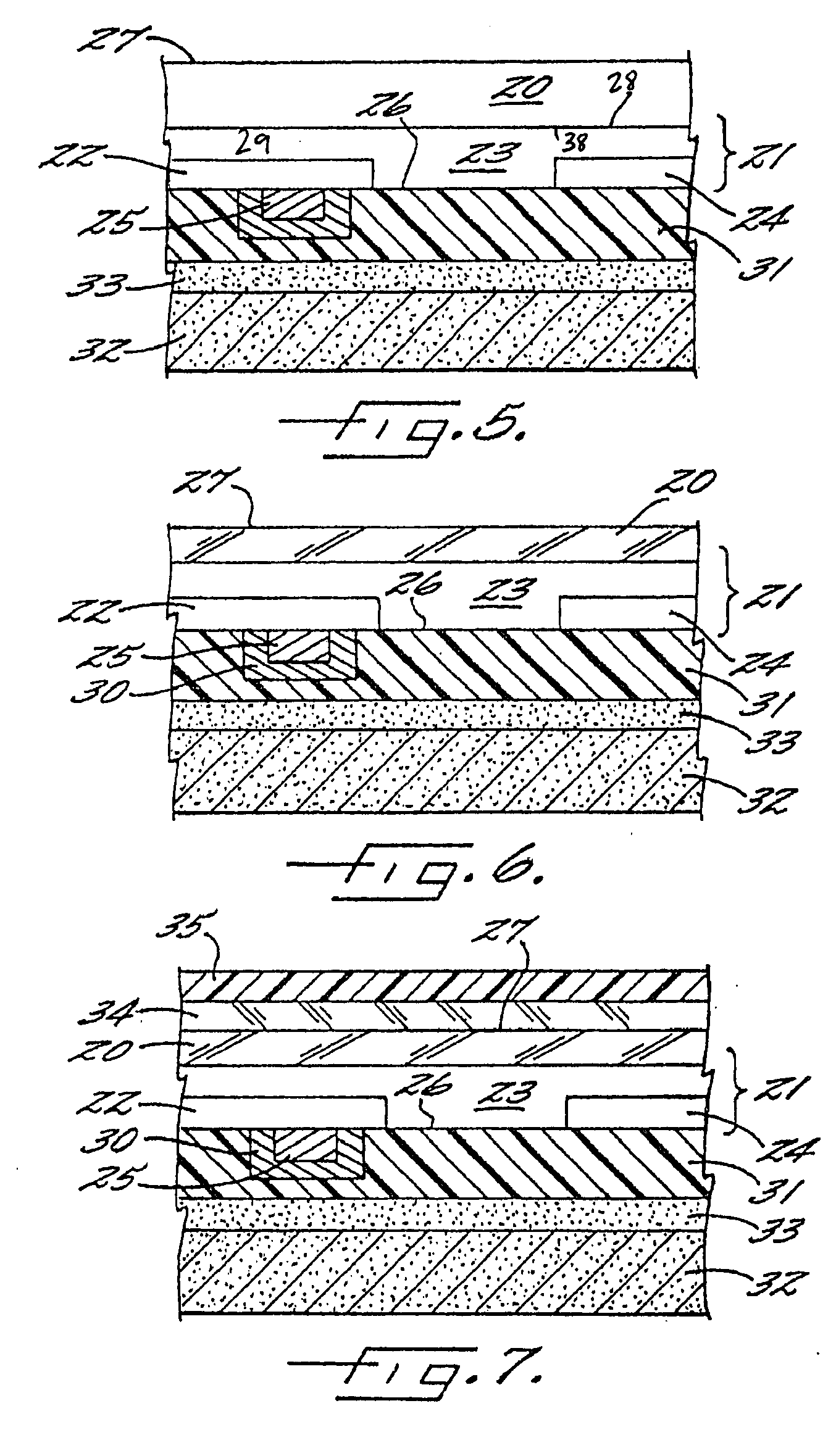
[0046]In a first aspect, the invention is a method of forming vias in particular materials—preferably, silicon carbide and Group III nitrides—that enables integrated circuits, and particularly monolithic microwave integrated circuits, to be formed on silicon carbide substrates with epitaxial layers on the substrate. The invention allows the devices to be connected to external circuitry in a manner that reduces the inductance problems that are characteristic of such MMICS when wire bonding is used to form electrical contacts for high frequency devices and circuits.

[0047]FIGS. 1 through 11 illustrate in sequential fashion the basic steps of the method aspects of the present invention. These will be described somewhat generally, following which particular experimental details will be set forth. Because much of the background of MMICs and their function is well understood in this art, these will not be described in particular detail other than as necessary to highlight the invention. In...


PUM


Abstract

A method of fabricating an integrated circuit on a silicon carbide substrate is disclosed that eliminates wire bonding that can otherwise cause undesired inductance. The method includes fabricating a semiconductor device in epitaxial layers on a surface of a silicon carbide substrate and with at least one metal contact for the device on the uppermost surface of the epitaxial layer. The opposite surface of the substrate is then ground and polished until it is substantially transparent. The method then includes masking the polished surface of the silicon carbide substrate to define a predetermined location for at least one via that is opposite the device metal contact on the uppermost surface of the epitaxial layer and etching the desired via in steps. The first etching step etches through the silicon carbide substrate at the desired masked location until the etch reaches the epitaxial layer. The second etching step etches through the epitaxial layer to the device contacts. Finally, metallizing the via provides an electrical path from the first surface of the substrate to the metal contact and to the device on the second surface of the substrate.

Description

[0001]This application is a continuation-in-part of Ser. No. 11 / 067,543, filed Feb. 25, 2005, now U.S. Pat. No. 7,125,786, which is a continuation in part of Ser. No. 10 / 249,448, filed Apr. 10, 2003, now U.S. Pat. No. 6,946,739, which is a continuation of Ser. No. 10 / 007,431, filed Nov. 8, 2001, now U.S. Pat. No. 6,649,497, which is a continuation of Ser. No. 09 / 546,821 filed Apr. 11, 2000, now U.S. Pat. No. 6,475,889.STATEMENT REGARDING FEDERALLY SPONSORED RESEARCH AND DEVELOPMENT[0002]This invention was developed under DARPA Contract No. F33615-96-C-1967. The government may have certain rights in this invention.BACKGROUND[0003]The present invention relates to integrated circuits formed in semiconductor materials and in particular relates to methods for forming via openings in semiconductor substrates, Group III nitride epitaxial layers, and the resulting structures. More particularly, the invention relates to the use of such vias to form monolithic microwave integrated circuits (M...

Claims


Application Information

Patent Timeline
IPC IPC(8): H01L21/335H01L21/768
CPCH01L21/76898H01L29/1608H01L29/2003H01L29/812H01L29/452H01L29/7787H01L29/4175H01L21/30604H01L21/3081H01L21/445
Inventor RING, ZOLTANSHEPPARD, SCOTT THOMASHAGLEITNER, HELMUT
Owner WOLFSPEED INC
Why Eureka
Try Eureka