Methods and system for analysis and management of parametric yield

a parametric yield and parametric technology, applied in the field of methods, can solve the problems of random defect yield loss due to yield loss, random defect yield loss in successive technology generation, process limited yield loss, etc., and achieve the effect of improving the accuracy of the process model

Inactive Publication Date: 2009-04-23
MENTOR GRAPHICS CORP
View PDF4 Cites 258 Cited by
  • Summary
  • Abstract
  • Description
  • Claims
  • Application Information

AI Technical Summary

Benefits of technology

[0123]fitting discrepancy between the measured temperature distribution mapand at least one of the spatial distribution of on-current and the spatial distribution of off-current to improve accuracy of the process model.

Problems solved by technology

Random defect yield loss is the yield loss due to random defects generated during manufacturing of a semiconductor chip.
As feature sizes shrink in a semiconductor chip, functionality of the semiconductor chip is more readily disturbed by random defects generated during semiconductor processing steps, resulting in increased in the random defect yield loss in successive technology generation.
Process limited yield loss is the yield loss due to failure to control process parameters within specification.
Process limited yield loss is thus due to an out-of-specification process parameter such as a thickness of a film, recess depth of a structure in a semiconductor substrate, and composition of a material.
Inherent variability in semiconductor manufacturing processes causes some semiconductor chips to be out-of-specification for at least one process parameter.
If the out of spec condition results in a short or open due then the chip is said to suffer from Process limited yield.
Note, not all out of spec process parameters result in process limited yield.
Increase in complexity of processing steps contributes to increase in the process limited yield loss, while improvement in process control tends to mitigate the impact of the processing steps on the process limited yield.
Parametric yield loss is the yield loss due to the fraction of manufactured semiconductor chips that do not meet performance specifications among the chips that do not suffer from random defect yield loss or process limited yield loss.
If an out of spec process parameter does not result in a hard failure, such as a short or an open, but does contribute to a deviation from modeled simulated behavior, and this deviation contributes to the chip not meeting the performance specification, then the chip is said to suffer from parametric or circuit limited yield.
Additionally, at least one of design specification for the chip, which may be, for example, circuit timing or power consumption in on-state or in off-state, is out of specification.
The cause of the failure of the chip to meet the design specification may not be attributed to the random defect yield loss or process limited yield loss, but is attributed to statistical distribution of performance of individual semiconductor devices in the semiconductor chip.
While being a useful concept, design for manufacturability does not provide algorithms or methodology for systematically increasing parametric yield.
It should be recognized, however, that employing an aggressive design that may potentially cause parametric yield issues is necessary to design a high performance chip.
The difficult part is to estimate the balance between a potential gain in performance of an aggressive design and increase in parametric yield, i.e., decrease in parametric yield loss, of a conservative design.
Further, nominal leakage currents are estimated to specify power consumption of the chip.
In this case, few courses of systematic action are available to the semiconductor chip manufacturing facility for investigation of the source of the depressed parametric yield.
While some methods are known in the art for diagnosing depressed process limited yield such as sorting the semiconductor chips by processing history or process variations, depressed parametric yield is much more difficult to investigate since the depressed parametric yield is correlated to specific design features of the semiconductor chip.
In financial perspective, when a semiconductor chip manufacturing facility commits to manufacture semiconductor chips based on an unknown chip design, the level of parametric yield loss is unpredictable from the perspective of the semiconductor chip manufacturing facility, while a customer generating a new chip design may have a vague idea of the level of expected parametric yield.
Thus, lack of precise estimation of the parametric yield on the new chip design exposes a semiconductor chip manufacturing facility to a financial uncertainty, while the customer submitting the new design is not provided with any guidance on how to improve the design to enhance the parametric yield.

Method used


Image

  • Methods and system for analysis and management of parametric yield
  • Methods and system for analysis and management of parametric yield
  • Methods and system for analysis and management of parametric yield

Examples


Embodiment Construction

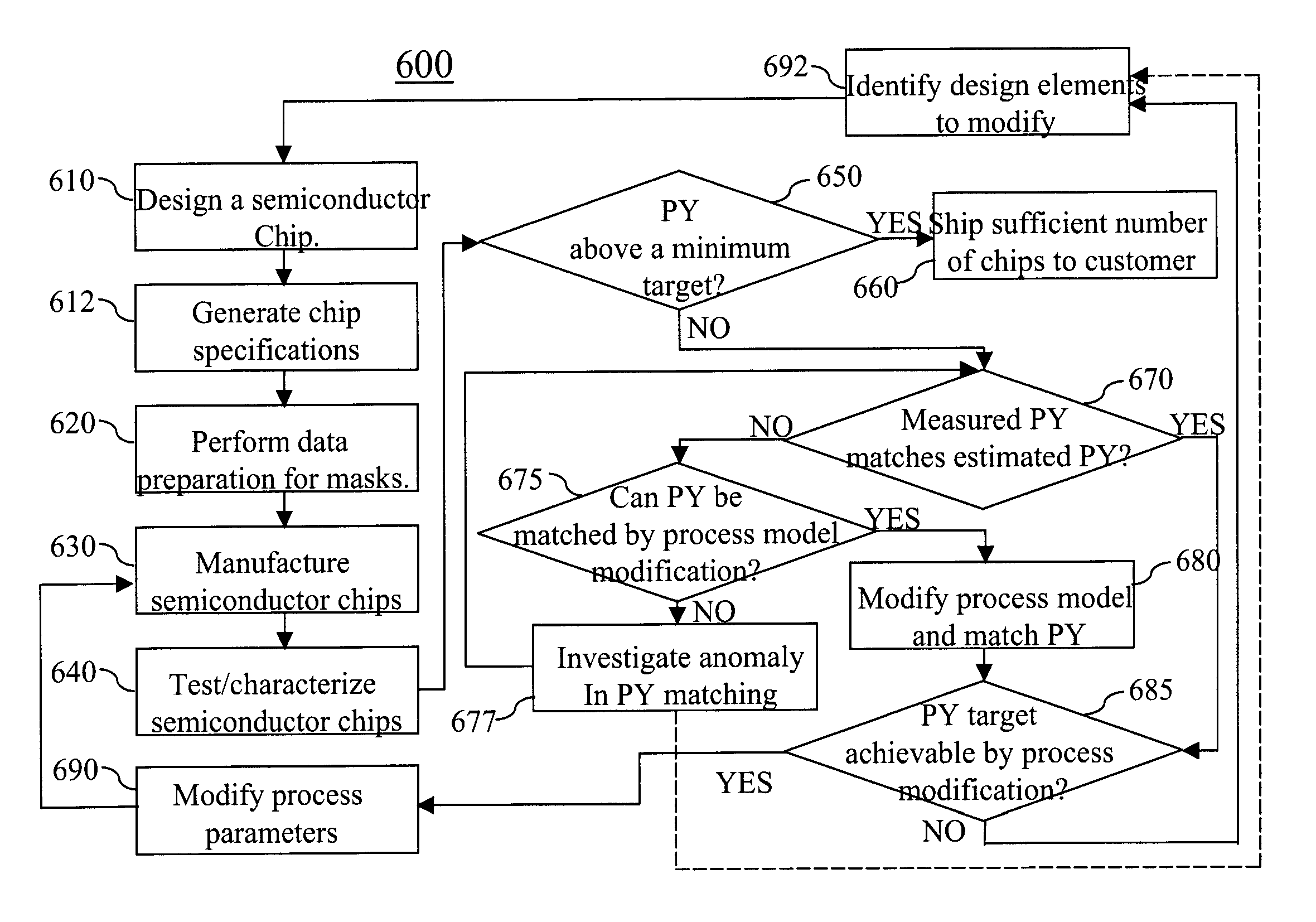
[0134]As stated above, the present invention relates to methods and systems for analyzing and improving parametric yield in semiconductor device manufacturing, which are now described in detail with accompanying figures. It is noted that like and corresponding elements mentioned herein and illustrated in the drawings are referred to by like reference numerals.

[0135]In a transistor, the distance between source and drain regions of the transistor and an edge of a well containing the source and drain regions affects the threshold voltage of the transistor. Such effects are known in the art as well proximity effects. U.S. Pat. No. 7,089,513 to Bard et al. describes well proximity effects and is herein incorporated by reference.

[0136]Due to well proximity effects, threshold voltages of the p-type field effect transistors of the same category that differ only by the size, i.e., the width of the gate that is the dimension of an active area abutting a gate dielectric along the direction per...


PUM


Abstract

Impact on parametric performance of physical design choices for transistors is scored for on-current and off-current of the transistors. The impact of the design parameters are incorporated into parameters that measure predicted shift in mean on-current and mean off-current and parameters that measure predicted increase in deviations in the distribution of on-current and the off-current. Statistics may be taken at a cell level, a block level, or a chip level to optimize a chip design in a design phase, or to predict changes in parametric yield during manufacturing or after a depressed parametric yield is observed. Further, parametric yield and current level may be predicted region by region and compared with observed thermal emission to pinpoint any anomaly region in a chip to facilitate detection and correction in any mistakes in chip design.

Description

FIELD OF THE INVENTION[0001]The present invention relates to methods and systems for analyzing and improving parametric yield in semiconductor device manufacturing.BACKGROUND OF THE INVENTION[0002]With continual scaling of dimensions in semiconductor devices and increase in the number of gates per chip, yield management in semiconductor manufacturing has become critical for economical and profitable operation of chip manufacturing facilities. Referring to FIG. 1, past trends up to 65 nm technology node and forecast for future technology nodes show three components of yield loss including random defect yield loss, process limited yield loss, and parametric yield loss.[0003]Random defect yield loss is the yield loss due to random defects generated during manufacturing of a semiconductor chip. As feature sizes shrink in a semiconductor chip, functionality of the semiconductor chip is more readily disturbed by random defects generated during semiconductor processing steps, resulting in ...

Claims


Application Information

Patent Timeline
Patent Type & Authority Applications(United States)
IPC IPC(8): G06F9/45
CPCG01R31/26G06F17/5045G06F30/30
Inventor CULP, JAMES A.CHANG, PAULCHIDAMBARRAO, DURESETIELAKKUMANAN, PRAVEENHIBBELER, JASONMOCUTA, ANDA C.
Owner MENTOR GRAPHICS CORP
Why Eureka
Try Eureka