Electrically conductive structure of circuit board and circuit board using the same

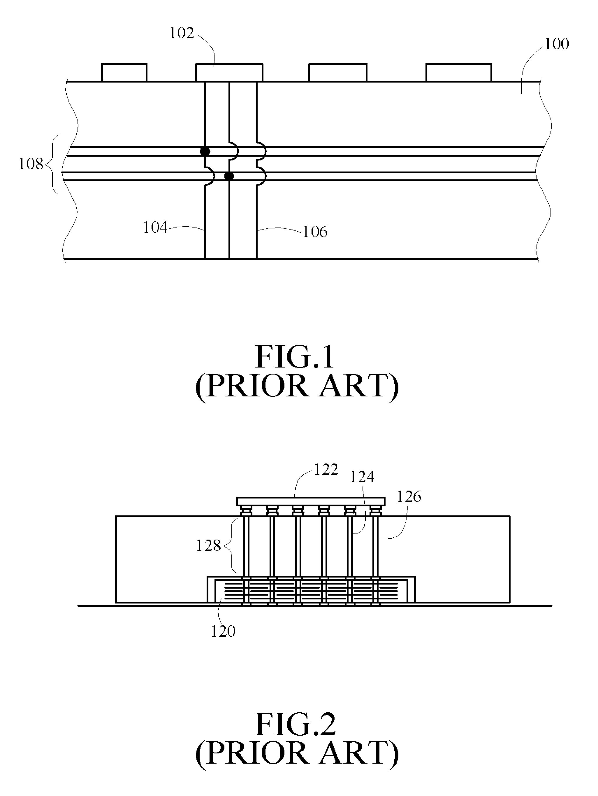
a technology of electrically conductive structure and circuit board, which is applied in the direction of cross-talk/noise/interference reduction, electrical apparatus contruction details, etc., can solve the problems of ineffective reduction of esl b>128/b> of feedthrough conductors marked at metal conductive structure in the drawing, unsatisfactory operation of electronic devices, and inability to effectively reduce esl b>128/b> of feedthrough

Active Publication Date: 2009-04-30
IND TECH RES INST
View PDF17 Cites 46 Cited by
  • Summary
  • Abstract
  • Description
  • Claims
  • Application Information

AI Technical Summary

Benefits of technology

[0010]Therefore, it is an urgent and bottleneck problem in need of a solution to reduce the impedance of the decoupling capacitor, as the operation frequency is higher than the self-resonant frequency, and increase the low impedance bandwidth of the decoupling capacitor so as to effectively reduce the simultaneous switching noises with the increase of the signal switching speed.

Problems solved by technology

Consequently, the power supply from the circuit board cannot provide a stable power at such a high switching speed, resulting in an unsatisfactory operation of the electronic device.
Moreover, a power noise or ground bounce may be induced in the power delivery systems.
Although the patent may reduce the ESL, the ESL 128 of the feedthrough conductors marked at the metal conductive structure in the drawing cannot be reduced effectively.
However, since the embedded planar capacitor is closer to the power and ground pins of the electronic device as compared with the SMD capacitor welded on the surface of the PCB or the IC substrate, the parasitic inductance produced on the power transmission path of the embedded capacitor at a high speed of signal switching is lower than that produced by the SMD capacitor.
But, similar to the common capacitor, along with the increasing signal switching speed of the electronic device of the planar capacitor, the parasitic inductance increases, resulting in degenerating the decoupling effect of the decoupling capacitor that is originally provided on the low-impedance path to depress the high-frequency undesired noises.

Method used


Image

  • Electrically conductive structure of circuit board and circuit board using the same
  • Electrically conductive structure of circuit board and circuit board using the same
  • Electrically conductive structure of circuit board and circuit board using the same

Examples


first embodiment

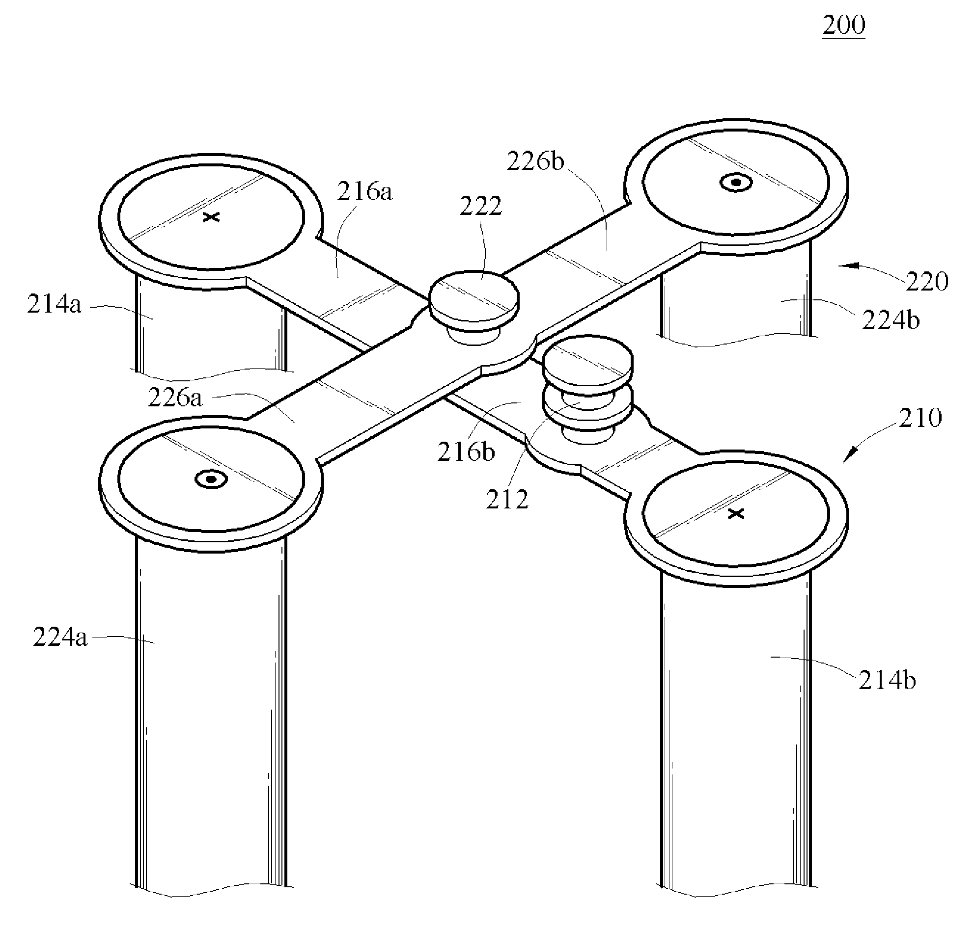
[0034]Referring to FIG. 5, FIG. 6 and FIG. 7, through the electrically conductive structure 200 of the first embodiment, at least one power contact 91 and at least one ground contact 92 of the electronic device 90 are electrically coupled to a power plane 302 and a ground plane 304 respectively in the circuit board 300. The electrically conductive structure 200 includes a first conductive structure 220 and a second conductive structure 210. The first conductive structure 220 has a first conducting section 222 electrically coupled to the power contact 91 at one end, and two (extending) first coupling sections 224a, 224b electrically connected to the first conducting section 222 at the other end. The two first coupling sections 224a, 224b are arranged in pairs, and the first coupling sections 224a, 224b are electrically connected to the power plane 302. The second conductive structure 210 has a second conducting section 212 electrically coupled to the ground contact 92 at one end, and...

second embodiment

[0046]FIG. 8 is a top view of the electrically conductive structure according to a Referring to FIG. 8, the electrically conductive structure 250 includes a first conductive structure 251 and a second conductive structure 255. The first conductive structure 251 has one first conducting section 252 and three first coupling sections 253a, 253b, 253c. The second conductive structure 255 has one second conducting section 256 and three second coupling sections 257a, 257b, 257c. The two first coupling sections 253a, 253b are arranged in pair, and the two second coupling sections 257a, 257b are also arranged in pairs. The two first coupling sections 253a, 253b in pairs and the two second coupling sections 257a, 257b in pairs are arranged in a staggered array, such that the effect of the magnetic flux cancellation may be achieved. The arrangement of the first coupling section 253c and the second coupling section 257c is not in pairs and not limited to that as shown in FIG. 8, and may be ac...

third embodiment

[0047]FIG. 9 shows the electrically conductive structure according to the present invention, which is applied in an electronic device having four power contacts and four ground contacts. Referring to FIG. 9, the electrically conductive structure 20 comprise four first conductive structures 21a, 21b, 21c, 21d and four second conductive structures 25a, 25b, 25c, 25d. Each first conductive structure 21a, 21b, 21c, 21d has one first conducting section 22a, 22b, 22c, 22d and two first coupling sections 23a, 24a, 23b, 24b, 23c, 24c, 23d, 24d. Each second conductive structure 25a, 25b, 25c, 25d also has one second conducting section 26a, 26b, 26c, 26d and two second coupling sections 27a, 28a, 27b, 28b, 27c, 28c, 27d, 28d. The four first conductive structures 21a, 21b, 21c, 21d and four second conductive structures 25a, 25b, 25c, 25d are not electrically connected. Actually, the four first conductive structures 21a, 21b, 21c, 21d are used to electrically connect the four power contacts of ...


PUM


Abstract

An electrically conductive structure includes a first conductive structure and a second conductive structure. Each has a conducting section at one end and a coupling section at the other end. The first and second conducting sections are electrically connected to a power and ground contact of an electronic device, respectively. The first and second coupling sections are respectively connected with power and ground layer of a circuit board. The first coupling sections are connected with the first conducting section through first extending sections and the second coupling sections are connected with the second conducting section through second extending sections. At least two coupling sections of the conductive structures are arranged in pairs. The first conductive structure and the second conductive structure are arranged in a staggered array to form two wiring loops having opposite current directions, thereby generating a magnetic flux cancellation effect.

Description

CROSS-REFERENCE TO RELATED APPLICATIONS[0001]This non-provisional application claims priority under 35 U.S.C. §119(a) on Patent Application No(s). 096140424 filed in Taiwan, R.O.C. on Oct. 26, 2007 the entire contents of which are hereby incorporated by reference.BACKGROUND OF THE INVENTION[0002]1. Field of Invention[0003]The present invention relates to an electrically conductive structure of a circuit board, and more particularly to a metal conductive structure disposed in a circuit board for electrically connecting a contact of an electronic device on the circuit board to a power layer and a ground layer of the circuit board. The discrete capacitor may be embedded in the circuit board.[0004]2. Related Art[0005]Usually, an electronic device is disposed on a printed circuit board (PCB) or an IC substrate (hereinafter a circuit board is taken as an example, but the present invention is not limited to the circuit board). The specific contact of the electronic device is electrically c...

Claims


Application Information

Patent Timeline
Patent Type & Authority Applications(United States)
IPC IPC(8): H05K1/11
CPCH01L2224/16225H05K1/0228H05K1/0231H05K1/0263H05K1/112H05K1/162H05K2201/10734H05K3/429H05K3/4602H05K2201/09245H05K2201/09627H05K2201/09709H05K1/185H01L2224/05568H01L2224/05573H01L2924/00014H01L2224/05599
Inventor HSU, CHIEN-MINWU, SHIH-HSIENLAI, SHINN-JUHLEE, MIN-LIN
Owner IND TECH RES INST
Why Eureka
Try Eureka