Infrared light source

Inactive Publication Date: 2009-04-30
YOKOGAWA ELECTRIC CORP
View PDF12 Cites 2 Cited by
  • Summary
  • Abstract
  • Description
  • Claims
  • Application Information

AI Technical Summary

Benefits of technology

[0017]Exemplary embodiments of the present invention provide a infrared light source which realize a highly-reliable device at low cost by imparting the function of a package to the device itself.
[0036]The infrared light source of the present invention does not require a package. Hence, cost equivalent to the cost of the package can be curtailed, and cost required to assemble the package can also be lessened. Hence, lower cost can be fulfilled. Further, the infrared light source can be mounted directly on a printed board, or the like, by means of soldering.
[0037]A highly-reliable sealing structure made by anodic-bonding can be implemented.
[0038]Further, quick dissipation of heat by way of the feedthrough electrodes enables implementation of high-speed blinking.

Problems solved by technology

In a case where the device shown in FIG. 6A is actually used, when the device is activated in the atmosphere, the reliability of the device deteriorates on account of a progress in oxidation, the corrosion of aluminum electrodes, intrusion of dust, and the like.
In relation to the package, consideration must be given to a window through which infrared radiation is emitted, hermeticity, exhaust heat, and the like, which becomes a contributor to domination of the cost and reliability of the device.

Method used


Image

  • Infrared light source
  • Infrared light source
  • Infrared light source

Examples


first embodiment

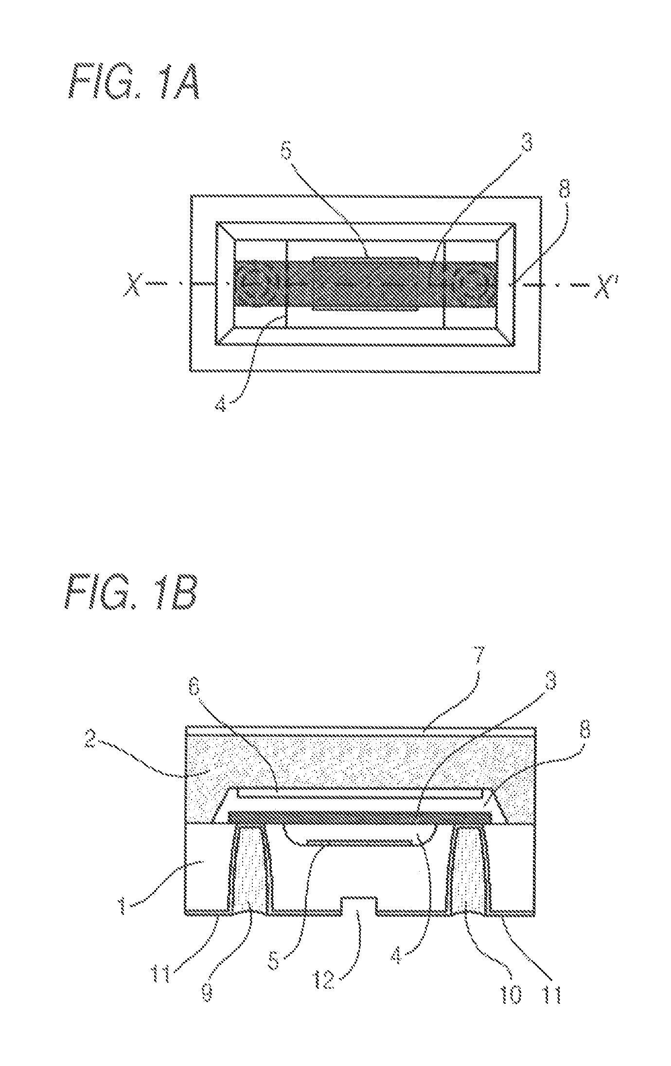
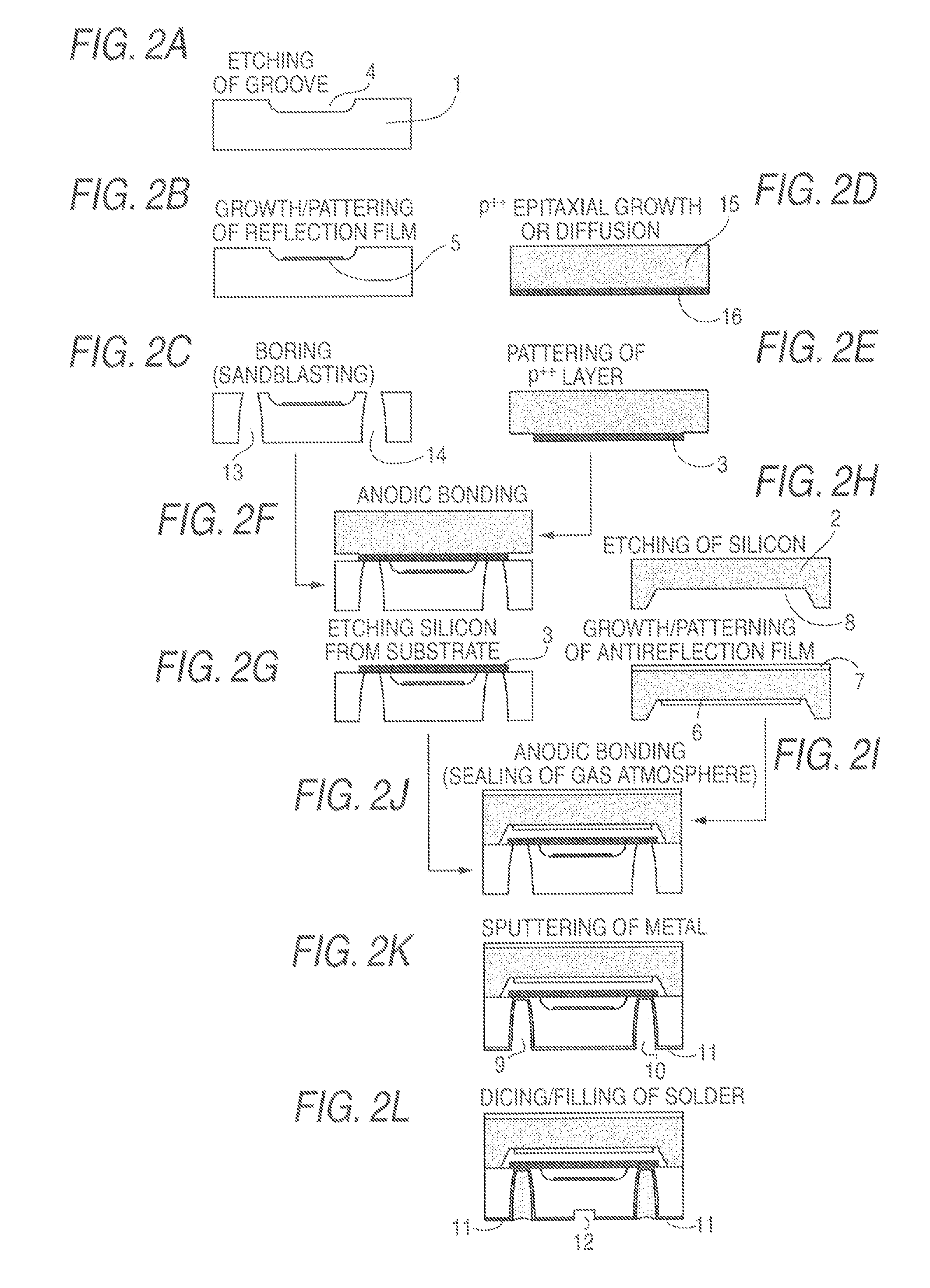
[0047]FIGS. 1A and 1B are structural drawings showing an embodiment of the infrared light source of the present invention. FIG. 1A is a plan view of the infrared light source of the present invention, and FIG. 1B is a cross-sectional view X-X′ shown in FIG. 1A.

[0048]A Pyrex (registered trademark) glass substrate is used as a first substrate (hereinafter called a “glass substrate 1”).

[0049]As shown in FIGS. 1A and 1B, in relation to the infrared light source, a silicon filament 3 is fabricated on the surface of the glass substrate 1. Feedthrough electrodes 9 and 10 are formed in the glass substrate 1.

[0050]The silicon filament 3 is fixed to areas of the glass substrate 1 corresponding to both ends of a recess (taken as a “recess 4 serving as a space located below the filament”) supporting the filament over a hollow space, by means of processing an area located below the filament.

[0051]In relation to the feedthrough electrodes 9 and 10, both ends of the silicon filament 3 are connecte...

second embodiment

[0078]FIGS. 3A and 3B are schematic views showing another embodiment of the infrared light source of the present invention. FIG. 3A is a plan view of the other embodiment of the infrared light source of the present invention, and FIG. 3B is a cross-sectional view taken along line X-X′ shown in FIG. 3A. In the drawings, elements analogous to those shown in FIGS. 1A and 1B are assigned the same reference numerals.

[0079]The structure shown in FIGS. 1A and 1B cannot be applied to the light source that requires a wide wavelength transmission band. Accordingly, FIGS. 3A and 3B show a structure to which a window material having a wide transmission wavelength band, such as calcium fluoride (CaF2), is to be bonded.

[0080]The Pyrex (registered trademark) glass substrate is used as the first substrate (hereinafter taken as a “glass substrate 1”).

[0081]As shown in FIGS. 3A and 3B, in the infrared light source, the silicon filament 3 is fabricated on the surface of the glass substrate 1. The feed...


PUM


Abstract

An infrared light source has a filament fabricated on a first substrate in the shape of a microbridge and energizes the filament so as to generate heat, thereby causing the filament to emit infrared radiation. The infrared light source has a second substrate that is bonded to the first substrate and seals the filament, and feedthrough electrodes that lead electrodes of the filament to the outside of the first substrate. Thereby, the function of the package is imparted to the device itself, to thus realize a highly-reliable device at low cost.

Description

TECHNICAL FIELD[0001]The present disclosure relates to an infrared light source employed in an infrared gas analyzer that measures a gas concentration in the atmosphere by use of infrared radiation.RELATED ART[0002]A non-dispersive Infrared gas analyzer (hereinafter referred to as an “NDIR gas analyzer”) which detects a rate of absorption by utilizing the fact that the wavelength of absorbed infrared radiation differs according to the type of a gas, to thus measure the concentration of a target gas, has been used for analyzing a gas.[0003]The NDIR gas analyzer introduces a gas to be measured into a cell whose dimensions are specified; radiates infrared light to the gas; and measures the concentration of the gas component on the basis of the amount of intensity attenuation of a specific infrared waveband. For instance, when carbon dioxide is measured, it is better to measure the amount of transmission of infrared radiation having a wavelength of 4.25 μm or thereabouts.[0004]FIG. 5 is...

Claims


Application Information

Patent Timeline
IPC IPC(8): H01K1/30H01K1/38
CPCH01K1/04H01K1/14H01K1/16H01K7/00H01K1/28H01K1/325H01K1/18
Inventor WATANABE, TETSUYAHARA, HITOSHIKISHI, NAOKI
Owner YOKOGAWA ELECTRIC CORP
Why Eureka
Try Eureka