
Silicon oxide film, method for forming silicon oxide film, and plasma CVD apparatus

a technology of silicon oxide film and silicon oxide film, which is applied in the direction of silicon oxide, plasma technique, silicon compounds, etc., can solve the problems of oxidation process not being performed, device adversely affected, charging damage generated, etc., and achieves high insulating properties, high quality, and dense structure.

Inactive Publication Date: 2011-08-25
TOKYO ELECTRON LTD
View PDF0 Cites 5 Cited by
  • Summary
  • Abstract
  • Description
  • Claims
  • Application Information

AI Technical Summary

Benefits of technology

[0019]According to a method for forming a silicon oxide film of the present invention, a high quality silicon oxide film (a silicon dioxide film or a silicon oxynitride film) having dense structure and high insulating properties can be formed by using a plasma CVD method.
[0020]Since a silicon oxide film obtained by the method of the present invention has dense structure and excellent insulating properties, and thus is high quality silicon oxide film, it can provide a highly reliable device. Accordingly, the method of the present invention has a high utility value in forming a silicon oxide film that is used as a gate insulation film or the like requiring high quality.

Problems solved by technology

However, when a multilayer insulation film is formed, the oxidation process cannot be performed, and it is required that is the multilayer insulation film is formed by depositing a silicon oxide film by using a CVD (Chemical Vapor Deposition) method.
Thus, there are problems that a device may be adversely affected due to increase of a thermal budget, and moreover, several restrictions may be generated when the device is manufactured.
Meanwhile, a plasma CVD method may be performed at a temperature around 500° C., but in this case, there is a problem that charging damage may be generated due to plasma having a high electron temperature (for example, Patent Document 1).
It has been difficult to form a film which satisfies these two requirements at the same time by a film-forming method using conventional plasma CVD.

Method used


Image

  • Silicon oxide film, method for forming silicon oxide film, and plasma CVD apparatus
  • Silicon oxide film, method for forming silicon oxide film, and plasma CVD apparatus
  • Silicon oxide film, method for forming silicon oxide film, and plasma CVD apparatus

Examples


Embodiment Construction

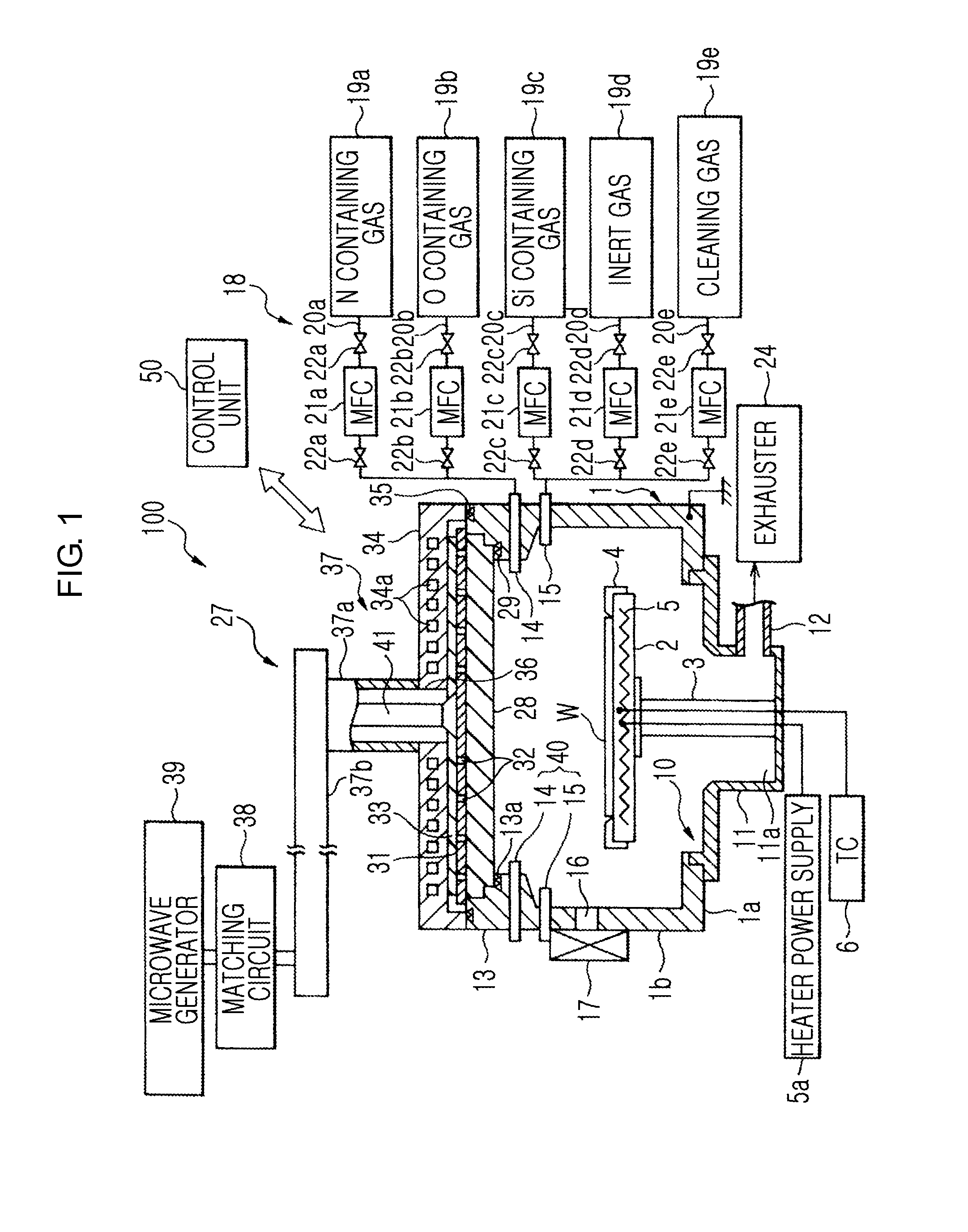
[0068]Hereinafter, the present invention will be described in detail by explaining exemplary embodiments of the invention with reference to the attached drawings. FIG. 1 is a schematic cross-sectional view showing a schematic configuration of plasma CVD apparatus 100 used for a method for forming a silicon oxide film of the present invention.

[0069]The plasma CVD apparatus 100 is an RLSA (Radial Line Slot Antenna) microwave plasma processing apparatus that can generate microwave excitation plasma having a high density and a low electron temperature, by introducing microwaves into a processing container through a planar antenna having a plurality of slots, specifically an RLSA and generating plasma. The plasma CVD apparatus 100 is able to perform a process using plasma having a low electron temperature from 0.7 eV to 2 eV, and a plasma density from 1×10¹⁰ / cm3 to 5×10¹² / cm3. Accordingly, the plasma CVD apparatus 100 may be very suitably used to form a silicon oxide film by plasma CVD i...


PUM

PropertyMeasurementUnit
Temperatureaaaaaaaaaa
Fractionaaaaaaaaaa

Abstract

To form a dense high-quality silicon oxide film (SiO2 film or SiON film) having excellent insulating properties and an etching rate below or equal to 0.11 nm / s when using a 0.5% dilute hydrofluoric acid solution, plasma CVD is performed by setting a pressure within the processing container in the range from 0.1 Pa to 6.7 Pa. and using a process gas containing an SiCl4 gas or an Si2H6 gas, and an oxygen gas, in a plasma CVD apparatus in which plasma is generated by introducing microwaves into a processing container through a planar antenna having a plurality of holes.

Description

TECHNICAL FIELD[0001]The present invention relates to a silicon oxide film, a method for forming the silicon oxide film, a computer readable recording medium used for the method, and a plasma CVD apparatus.BACKGROUND ART[0002]Currently, a thermal oxidation method, a plasma oxidation method, etc. that perform an oxidation process on silicon are known as methods of forming a high quality silicon oxide film (SiO2 film or SiON film) having high insulating properties. However, when a multilayer insulation film is formed, the oxidation process cannot be performed, and it is required that is the multilayer insulation film is formed by depositing a silicon oxide film by using a CVD (Chemical Vapor Deposition) method. In order to form a silicon oxide film having high insulating properties by using a CVD method, a high temperature process at a temperature from 600° C. to 900° C. is required. Thus, there are problems that a device may be adversely affected due to increase of a thermal budget, ...

Claims


Application Information

Patent Timeline
IPC IPC(8): C23C16/40C23C16/34C23C16/455C23C16/511C23C16/52C01B33/12
CPCC23C16/308C23C16/402C23C16/511H01L21/0214H01L21/31612H01L21/02211H01L21/02274H01L21/3145H01L21/02164
Inventor HONDA, MINORUNAKANISHI, TOSHIOKOHNO, MASAYUKIMIYAHARA, JUNYA
Owner TOKYO ELECTRON LTD
Learn More