Solar cell and method of manufacturing the same
- Summary
- Abstract
- Description
- Claims
- Application Information
AI Technical Summary
Benefits of technology
Problems solved by technology
Method used
Image

Examples
example 1
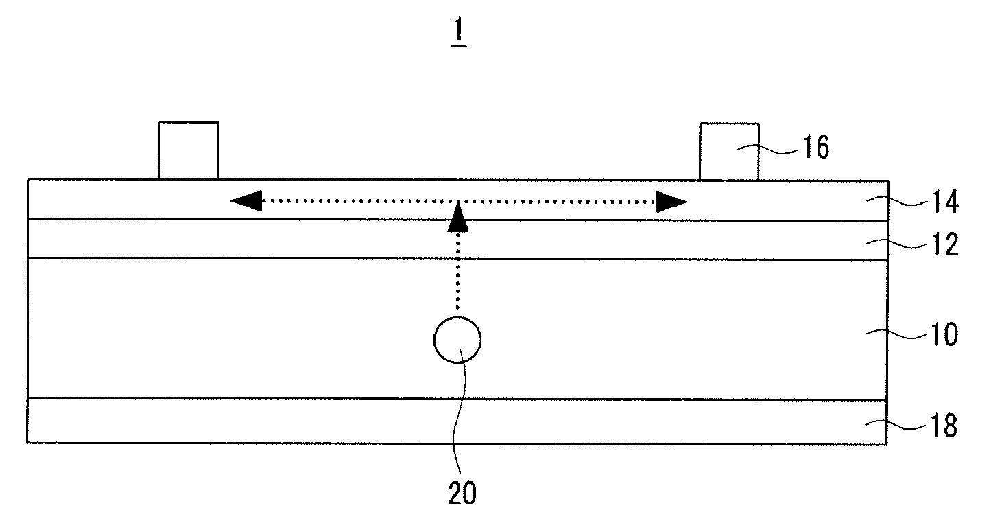
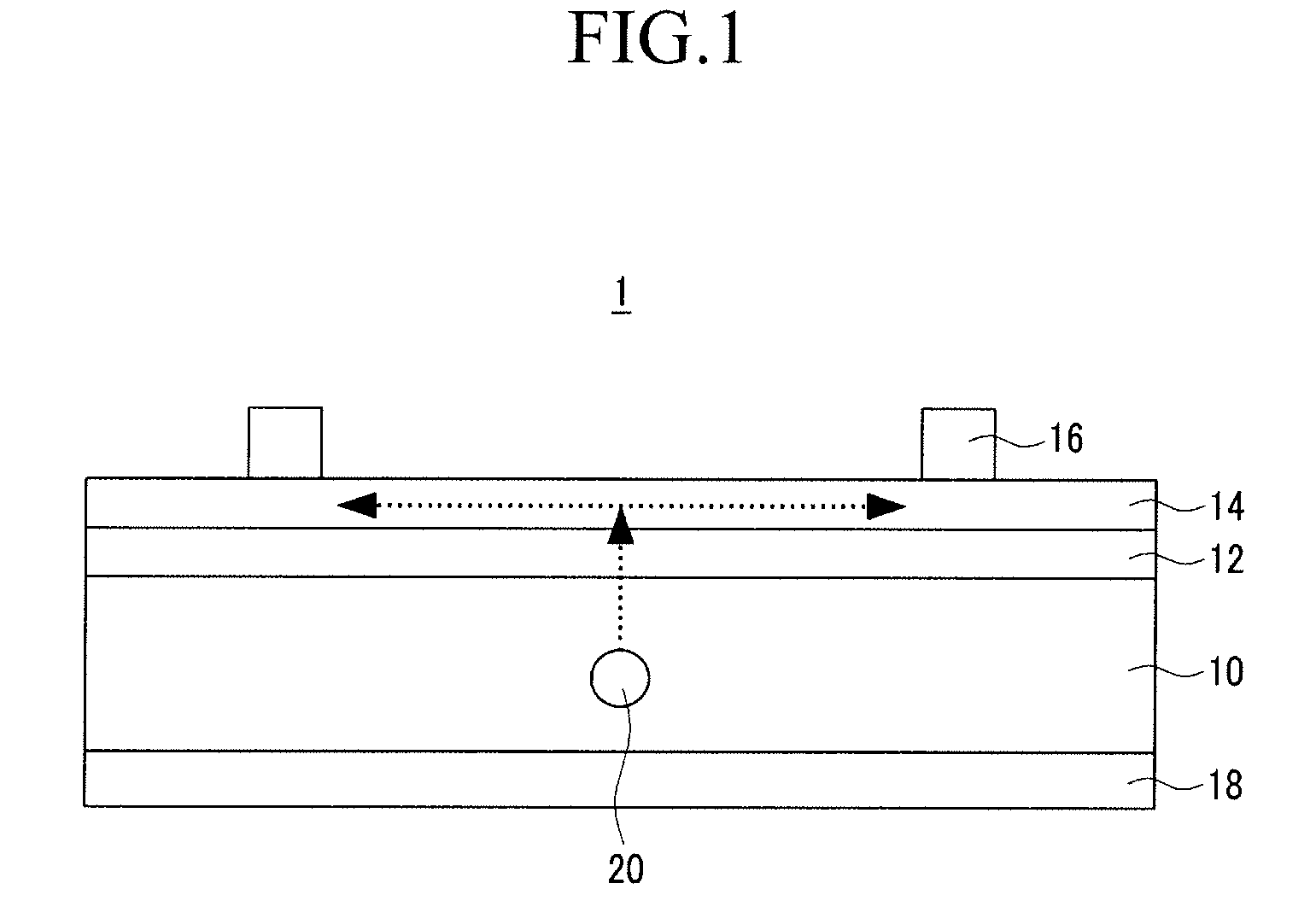
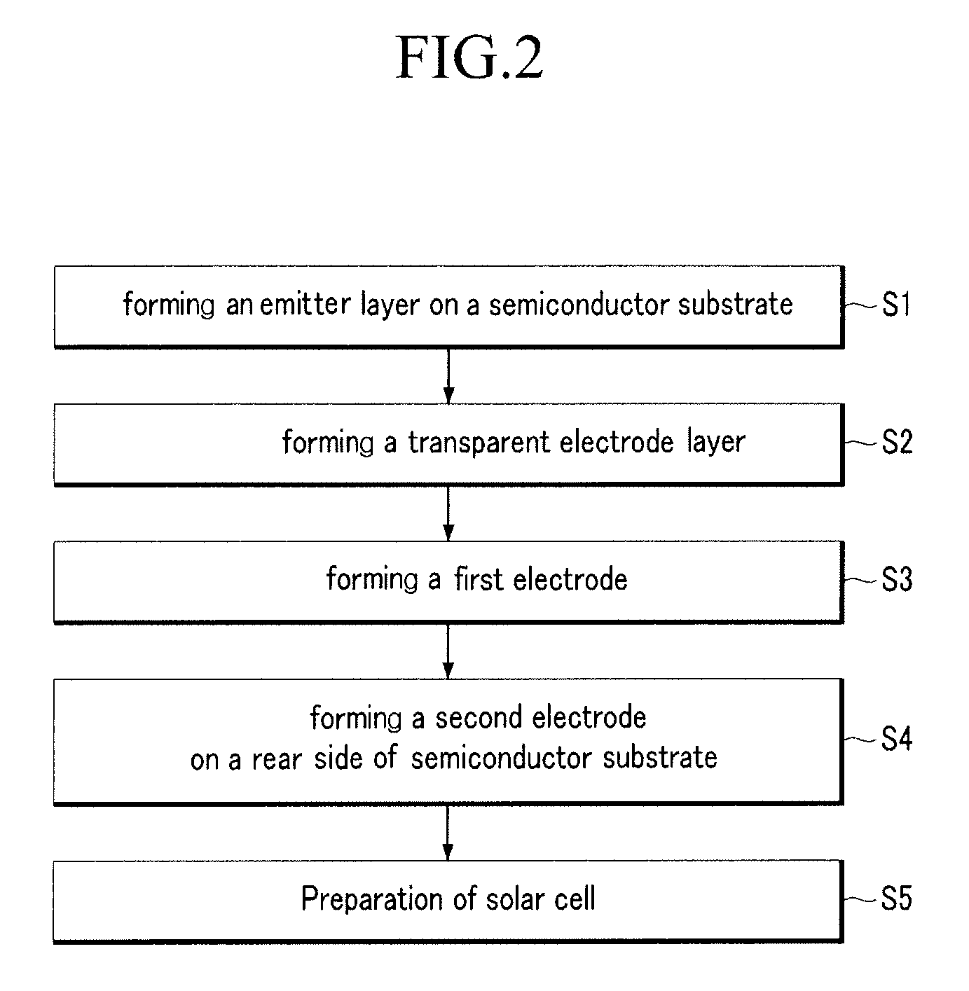
[0096]An emitter layer was disposed to be 0.45 μm thick on one side of a boron-doped p-type silicon substrate (specific resistance: 1 μΩ·cm) with phosphorus-doped n-type silicon. The boron was doped in an amount of 1.5×10¹⁶ / cm3 on a p-type silicon substrate. The emitter layer including n-type silicon had a surface resistance of 50Ω / □.
[0097]Then, an 80 nm-thick conductive transparent electrode layer was disposed on the emitter layer with a sputtering method.
[0098]An Al-containing paste was screen-printed on the other side of the p-type silicon substrate (i.e., on the side having no emitter layer). In addition, the p-type silicon substrate with the conductive transparent electrode layer was screen-printed with a Ag-containing paste every 6 mm to form a pattern, and thereafter sintered at 400° C. for 30 seconds to simultaneously (or concurrently) form first and second electrodes to thereby fabricate a solar cell.
[0099]The emitter layer in the corner of the solar cell was removed with a...
example 2
[0100]A 0.3 μm-thick emitter layer was disposed with phosphorus-doped n-type silicon on one side of a boron-doped p-type silicon substrate (specific resistance: 1 Ω·cm). Here, the boron was doped in an amount of 1.5×10¹⁶ / cm3 on the p-type silicon substrate. The emitter layer including n-type silicon had a surface resistance of 100Ω / □.
[0101]Then, a conductive transparent electrode layer was disposed to be 80 nm thick on the emitter layer by using indium tin oxide (ITO) with a sputtering method.
[0102]Further, an Al-containing paste was screen-printed on the other side of the p-type silicon substrate (i.e., on the side having no emitter layer). In addition, the p-type silicon substrate with the conductive transparent electrode layer was screen-printed with a Ag-containing paste every 2.5 mm to form a pattern, and thereafter sintered at 400° C. for 30 seconds to simultaneously (or concurrently) form first and second electrodes to thereby fabricate a solar cell.
[0103]The emitter layer in...
example 3
[0104]A 0.3 μm thick phosphorus-doped n-type silicon emitter layer was disposed on one side of a boron-doped p-type silicon substrate (specific resistance: 1 Ω·cm). Here, the boron was doped in an amount of 1.5×10¹⁶ / cm3 on the p-type silicon substrate. The emitter layer including n-type silicon had surface resistance of 100Ω / □.
[0105]Then, a conductive transparent electrode layer was disposed to be 80 nm thick on the emitter layer by using indium tin oxide (ITO) with a sputtering method.
[0106]An Al-containing paste was screen-printed on the other side of the p-type silicon substrate (i.e., on the side having no emitter layer). In addition, the p-type silicon substrate with the conductive transparent electrode layer was screen-printed with an Ag-containing paste every 6 mm to form a pattern, and thereafter, sintered at 400° C. for 30 seconds to simultaneously (or concurrently) form first and second electrodes to finally fabricate a solar cell.
[0107]The emitter layer in the corner of t...
PUM
 Abstract
Description
Claims
Application Information
 - R&D Engineer
- R&D Manager
- IP Professional
- Industry Leading Data Capabilities
- Powerful AI technology
- Patent DNA Extraction
Browse by: Latest US Patents, China's latest patents, Technical Efficacy Thesaurus, Application Domain, Technology Topic.
© 2024 PatSnap. All rights reserved.Legal|Privacy policy|Modern Slavery Act Transparency Statement|Sitemap