Method and Apparatus to Reduce Impedance Discontinuity in Packages

a technology of electronic circuits and discontinuities, applied in the field of electronic circuits, can solve the problems of increasing the opportunity for signal interference, reducing the quality of signals propagating through the interconnection of electronic packages, and reducing the quality of signals in electronic packages of these devices. the effect of reducing the discontinuity of signals

Inactive Publication Date: 2009-05-21
GLOBALFOUNDRIES INC
View PDF11 Cites 29 Cited by
  • Summary
  • Abstract
  • Description
  • Claims
  • Application Information

AI Technical Summary

Benefits of technology

[0008]In one embodiment PTH vias are fabricated with magnetic metal coatings to reduce distortion of high speed signals. Electronic packages output high speed signals that are compromised due to excess capacitance in PTHs. During fabrication of PTH vias, holes are drilled into the core dielectric material of the printed circuit board. Then, a magnetic metal coating is added to the walls of PTHs to reduce the impedance discontinuity of the electronic package. Deposition of a metal material, such as nickel, is followed by coating the metal material with copper. After coating the walls of the PTH via, resin may be deposited into the via.
[0009]In one embodiment, impedance discontinuity is reduced by utilizing a PTH via connected to the trace of a printed circuit board. The PTH via, coated with the magnetic metal coating, is connected to the trace from the copper layer of the PTH via. The magnetic coating material increases internal and external inductance in the electronic package by changing the magnetic environment. PTH vias with only a copper layer contain excess capacitance. Increasing the inductance of the PTH via utilizing the magnetic layer compensates for the excess capacitance without compromising the structure of the printed circuit board.
[0010]In another embodiment, impedance discontinuity is further reduced by utilizing one or more PTH vias that are not connected to the trace of a printed circuit board. A magnetic metal layer is deposited on the PTH vias, followed by the copper coating and resin deposition. However, one or more PTH vias are imbedded in the dielectric core of the printed circuit board without connecting to a trace. Additional PTH vias with metal coatings and no trace connection further increases inductance; thereby, reducing impedance discontinuity.

Problems solved by technology

When operating at high transmission rates, impedance discontinuity decreases the quality of signals in the electronic packages of these devices.
Also, excessive capacitance of plated through holes (PTHs) and ball grid arrays (BGAs) can significantly degrade the quality of signals propagating through interconnects of an electronic package.
Dramatically increasing the inductive trace increases the length the signal travels; thereby increasing opportunities for signal interference.
In addition to increased signal length, the intricate detail of the trace pattern may be impractical to integrate into a currently running process.
Removing the planar conductive layers above the BGA pads reduces capacitance; however, removing the planes also deteriorates the plane integrity of the printed circuit board of which the electric package is built.
In addition to jeopardizing the plane integrity, the routes in which the signals may travel are drastically decreased and the mechanical strength of the PCB is diminished.

Method used


Image

  • Method and Apparatus to Reduce Impedance Discontinuity in Packages
  • Method and Apparatus to Reduce Impedance Discontinuity in Packages
  • Method and Apparatus to Reduce Impedance Discontinuity in Packages

Examples


Embodiment Construction

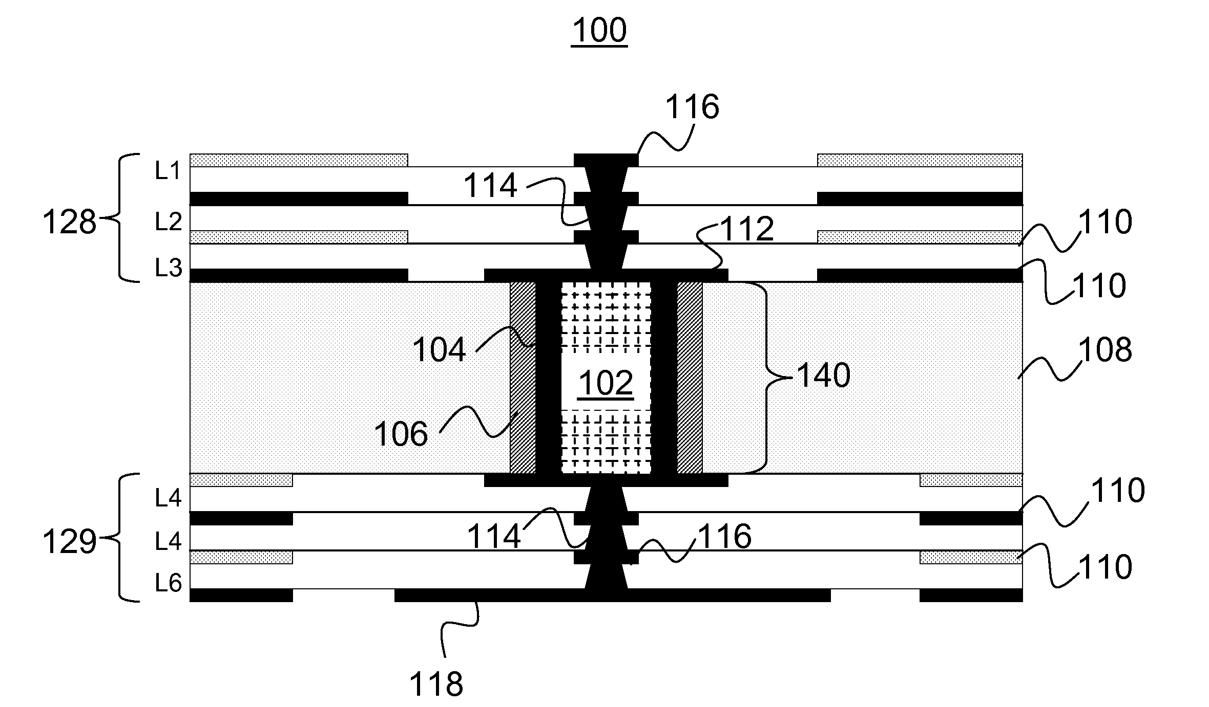
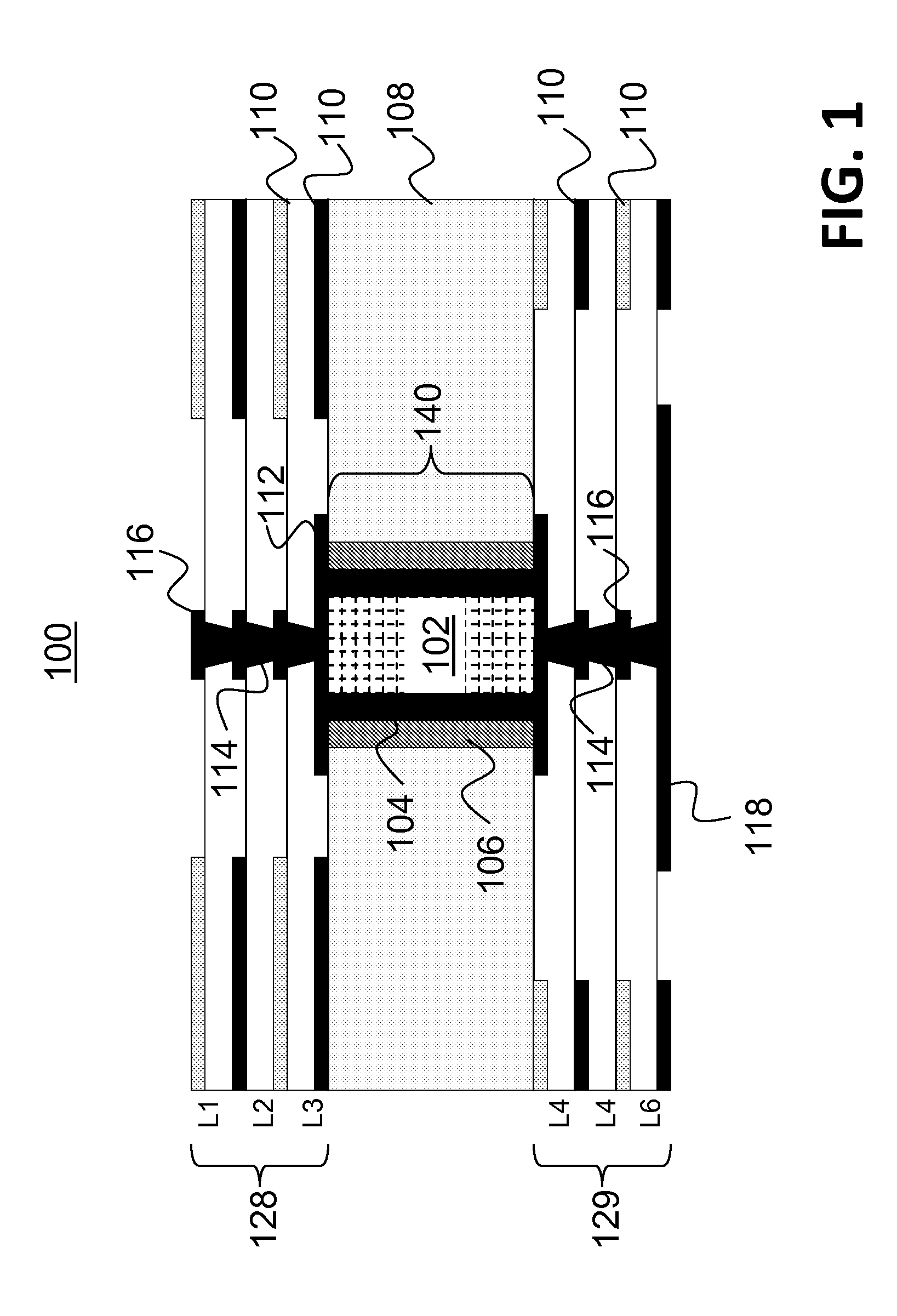
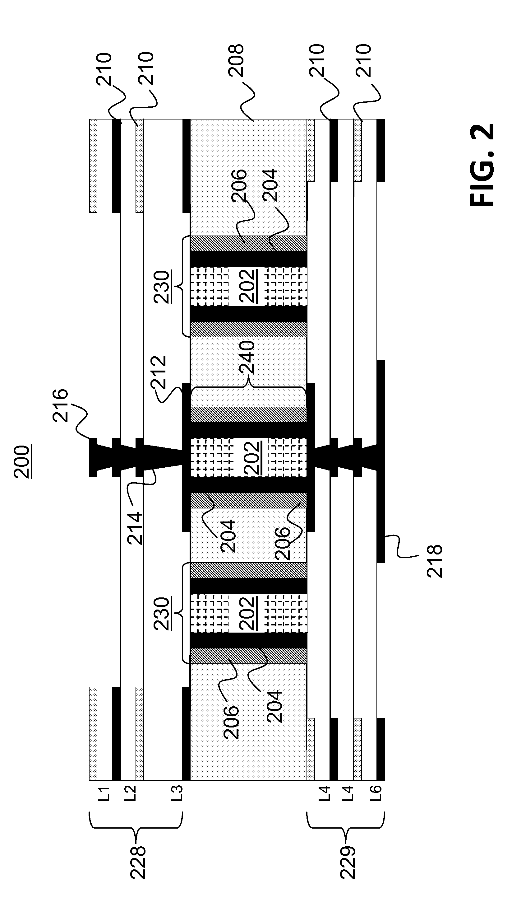
[0007]Disclosed are a method, system and apparatus for coating plated through holes (PTHS) to reduce impedance discontinuity in electronic packages. PTHs are coated with a magnetic metal material, such as nickel, to increase the internal and external inductance of the PTHs, thereby providing decreased impedance discontinuity of the signals in electronic packages. PTH vias are imbedded in the core of a printed circuit board comprising a core layer, a plurality of buildup layers, a plurality of micro-vias, and a plurality of traces. Traces electrically interconnect each of the micro-vias to PTH vias, forming an electrically conductive path.

[0008]In one embodiment PTH vias are fabricated with magnetic metal coatings to reduce distortion of high speed signals. Electronic packages output high speed signals that are compromised due to excess capacitance in PTHs. During fabrication of PTH vias, holes are drilled into the core dielectric material of the printed circuit board. Then, a magnet...


PUM

PropertyMeasurementUnit
diameteraaaaaaaaaa
conductiveaaaaaaaaaa
impedanceaaaaaaaaaa

Abstract

A method, system and apparatus for coating plated through holes (PTHs) to reduce impedance discontinuity in electronic packages. PTH vias are imbedded in the core of a printed circuit board comprising a core layer, a plurality of buildup layers, a plurality of micro-vias, and a plurality of traces. Traces electrically interconnect each of the micro-vias to PTH vias, forming an electrically conductive path. PTHs are coated with a magnetic metal material, such as nickel, to increase the internal and external conductance of the PTHs, thereby providing decreased impedance discontinuity of the signals in electronic packages.

Description

BACKGROUND[0001]1. Technical Field[0002]The present invention generally relates to electronic circuits and in particular to reducing impedance discontinuity in the packaging of electronic circuits.[0003]2. Description of the Related Art[0004]Electronic products, including computers, cellular telephones, and networking systems operate at ever increasing high transmission rates. When operating at high transmission rates, impedance discontinuity decreases the quality of signals in the electronic packages of these devices. Also, excessive capacitance of plated through holes (PTHs) and ball grid arrays (BGAs) can significantly degrade the quality of signals propagating through interconnects of an electronic package.[0005]Numerous techniques have been utilized to improve signal degradation in electronic packaging. For example, an intricate via pattern design, forming an extended, electrically conductive path, has been provided in an effort to decrease impedance discontinuity by increasing...

Claims


Application Information

Patent Timeline
Patent Type & Authority Applications(United States)
IPC IPC(8): H05K1/02H05K3/10
CPCY10T29/49165H05K2201/09536H05K3/42H05K3/4602H05K1/0233H05K1/115H05K1/112H05K2201/096H05K2201/086H01F17/0013
Inventor HARVEY, PAUL M.POWELL, DOUGLAS O.SAUTER, WOLFGANGZHOU, YAPING
Owner GLOBALFOUNDRIES INC
Why Eureka
Try Eureka