LED chip thermal management and fabrication methods
a technology of thermal management and fabrication methods, applied in the direction of electrolytic coatings, electrolysis coatings, liquid/solution decomposition chemical coatings, etc., can solve the problems of less satisfactory cte matching with leds, thermal expansion coefficient (cte) mismatch becomes an issue for device reliability, and the penetration rate is the lumen/$ cost of led lamps, etc., to achieve easy levelling, enhanced light extraction, and reduced cost of wafer bonding
- Summary
- Abstract
- Description
- Claims
- Application Information
AI Technical Summary
Benefits of technology
Problems solved by technology
Method used
Image

Examples
example 1
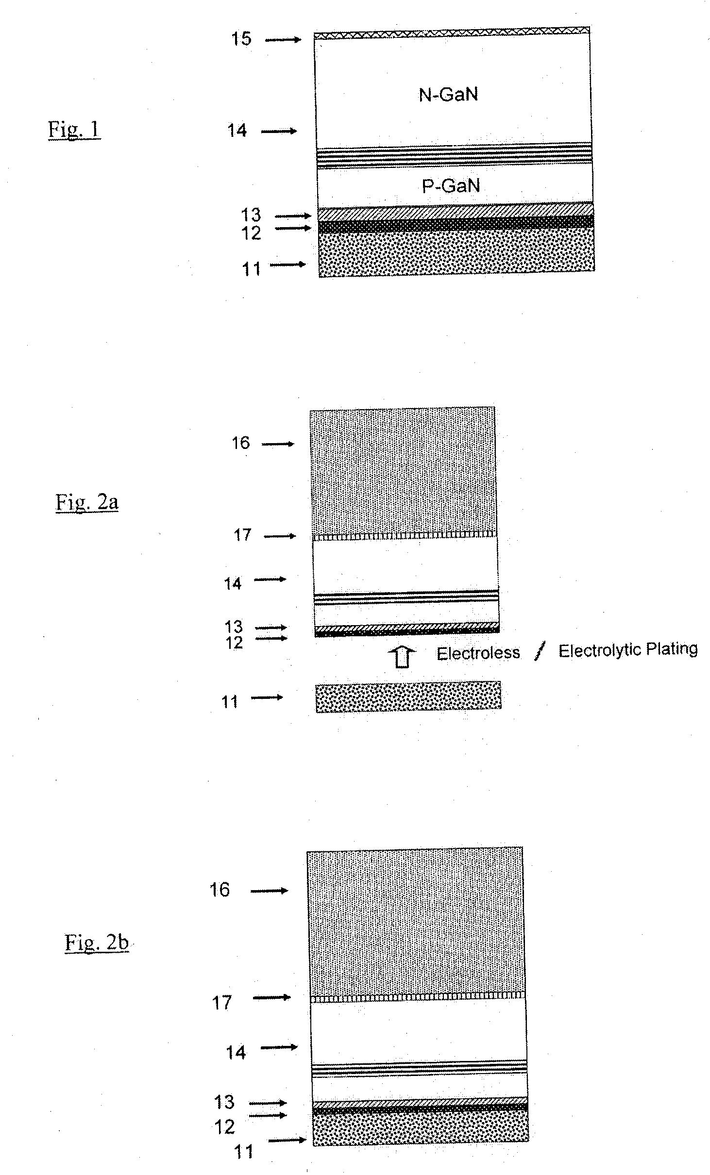
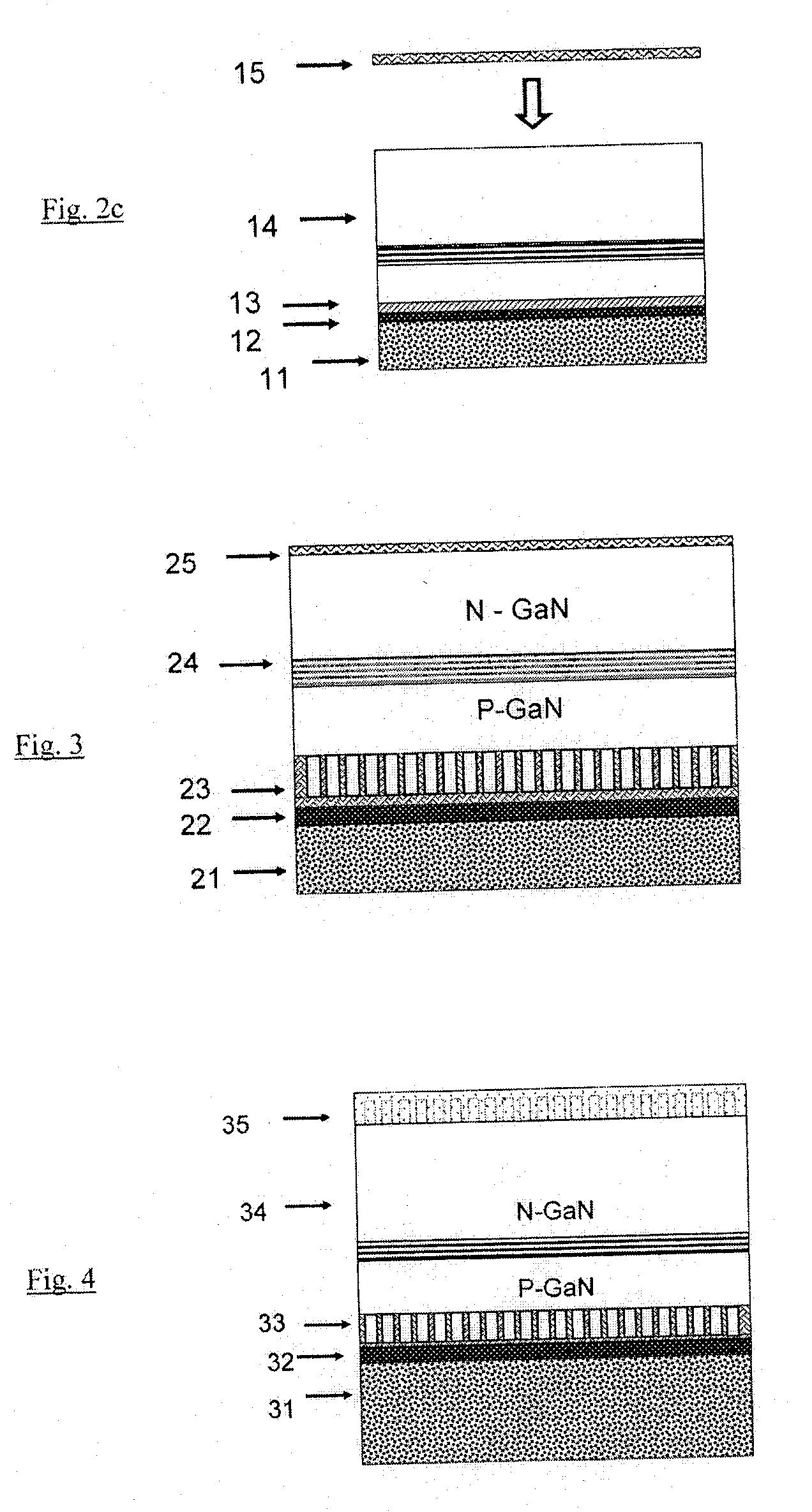
[0031]Although one embodiment of the invention is shown in FIGS. 1 and 2 above, it should be understood that this basic structure may be modified or combined with other improvements to further enhance the properties of the LEDs of the current invention. For example, FIG. 3 shows another exemplary structure of an embodiment of a vertical LED device with a foreign substrate removed. As above, the LED device includes an LED wafer or chip 24, a p-contact metal layer 23, a reflector layer 22, an electrolytically plated metal composite substrate 21 and an n-metal contact layer 25. A p-type bonding pad can be connected directly to the metal composite substrate 21, and an n-type bonding pad can be deposited on to the n-metal contact layer and connected by any suitable means. In the current embodiment to enhance light extraction, the p-type III-V nitride contact layer of wafer or chip 24 is roughened or patterned by various techniques. The roughened surface can be grown by in situ epitaxial ...
example 2
[0032]FIG. 4 shows another exemplary structure of an embodiment of a vertical LED device with a foreign substrate removed. Again, as in the first embodiment of the invention, the LED device includes an LED wafer or chip 34, a p-contact metal layer 33, a reflector layer 32, an electrolytically plated metal composite substrate 31 and an n-metal contact layer 35. A p-type bonding pad can be connected directly to the metal composite substrate 31, and an n-type bonding pad can be deposited on to the n-metal contact layer and connected by any suitable means. In this embodiment to enhance light extraction, both the p-type and n-type III-V nitride contact layers of wafer or chip 34 are roughened or patterned by various techniques. The roughened surface can be grown by in situ epitaxial growth with higher p-type doping. The roughened surface of the p- and n-type III-V nitrides can also be fabricated by wet etching, electrochemical etching or photochemical etching. The patterned surface can b...
example 3
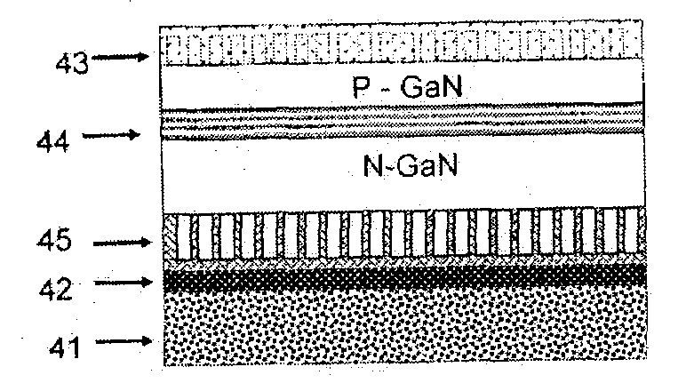
[0033]FIG. 5 shows another exemplary structure of an embodiment of an n-side down vertical LED device with a foreign substrate removed. In this embodiment, the LED device includes an LED wafer or chip 44, a transparent p-contact metal layer 43, an n-metal contact layer 45, a reflector layer 42 and an electrolytically plated metal composite substrate 41. An n-type bonding pad can be connected directly to the metal composite substrate 41 and a p-type bonding pad can be deposited on to the p-metal contact layer and connected by any suitable means. Again, to enhance light extraction, both the n-type and p-type III-V nitride contact layers of wafer or chip 44 may be roughened or patterned by various techniques. The p-type roughened surface can be grown by in situ epitaxial growth with higher p-type doping. The roughened surface of the p- and n-type III-V nitrides can also be fabricated by wet etching, electrochemical etching or photochemical etching. The patterned surface can be fabricat...
PUM
| Property | Measurement | Unit |
|---|---|---|
| Size distribution | aaaaa | aaaaa |
| Electrical conductor | aaaaa | aaaaa |
| Wavelength | aaaaa | aaaaa |
Abstract
Description
Claims
Application Information
 - Generate Ideas
- Intellectual Property
- Life Sciences
- Materials
- Tech Scout
- Unparalleled Data Quality
- Higher Quality Content
- 60% Fewer Hallucinations
Browse by: Latest US Patents, China's latest patents, Technical Efficacy Thesaurus, Application Domain, Technology Topic, Popular Technical Reports.
© 2025 PatSnap. All rights reserved.Legal|Privacy policy|Modern Slavery Act Transparency Statement|Sitemap|About US| Contact US: help@patsnap.com