Method of manufacturing a semiconductor device and processing apparatus

Active Publication Date: 2009-05-21
NTT MOBILE COMM NETWORK INC
View PDF9 Cites 22 Cited by
  • Summary
  • Abstract
  • Description
  • Claims
  • Application Information

AI Technical Summary

Benefits of technology

[0017]According to the manufacturing method of the semiconductor device and the processing apparatus of the present invention, deposits incl

Problems solved by technology

Thus, it can make a possible guess that an increase of a cost of the processing apparatus and consequently the manufacturing cost of the semiconductor device will be resulted in some

Method used


Image

  • Method of manufacturing a semiconductor device and processing apparatus
  • Method of manufacturing a semiconductor device and processing apparatus
  • Method of manufacturing a semiconductor device and processing apparatus

Examples


Example

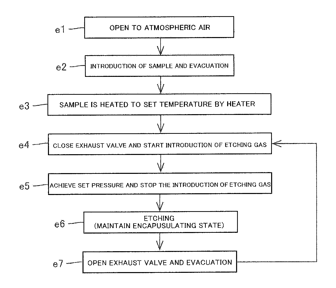
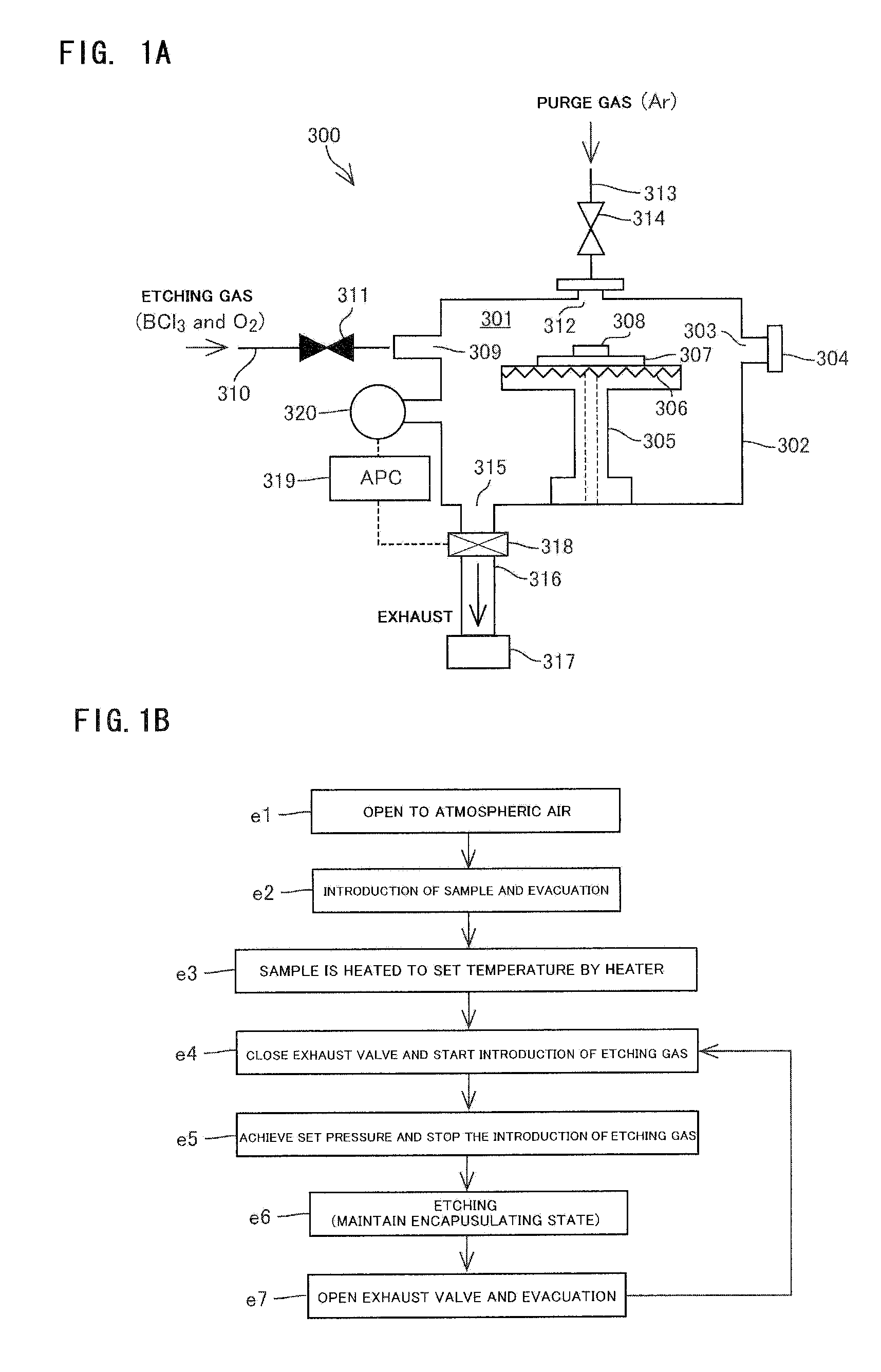
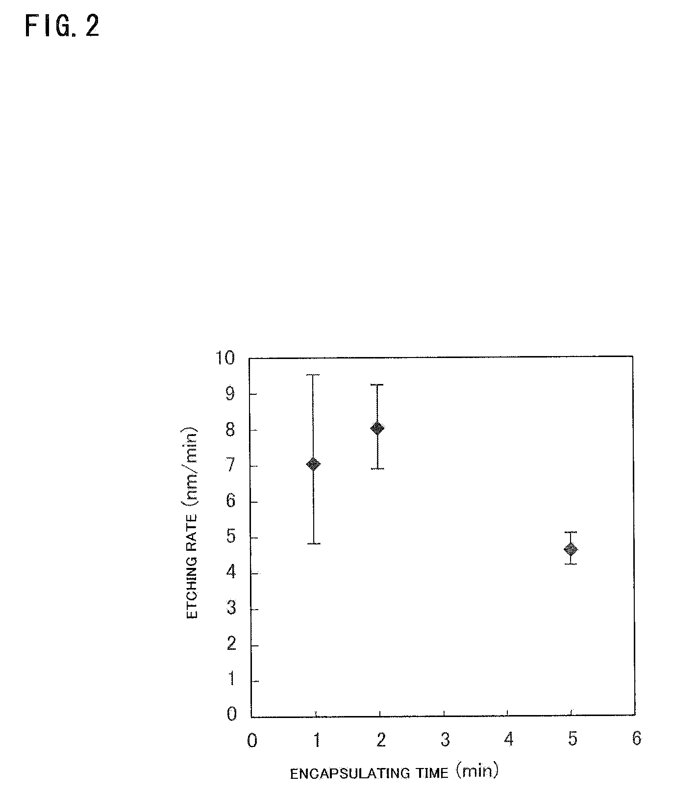
[0029]As described above, in some cases, a high etching rate is difficult to achieve with thermal etching. Inventors of the present invention make strenuous efforts in studying on a method of increasing the etching rate in thermal etching. As a result, based on the knowledge, the inventors of the present invention achieves a technique that the etching rate in thermal etching can be increased, by setting etching conditions such as oxygen-based gas concentration in the etching gas, temperature of the inside of the processing chamber (in a precise sense, temperature of a surface to be etched), and pressure in the processing chamber, in a prescribed range.

[0030]Thus, based on this knowledge, inventors of the present invention achieve the invention of a method of manufacturing a semiconductor device including the steps of: loading a substrate into a processing chamber; supplying processing gas into the processing chamber and depositing a high dielectric constant film on the substrate; un...


PUM

PropertyMeasurementUnit
Temperatureaaaaaaaaaa
Fractionaaaaaaaaaa

Abstract

To remove the deposit including a high dielectric constant film deposited on an inside of a processing chamber, by using a cleaning gas activated only by heat. The method includes the steps of: loading a substrate or a plurality of substrates into the processing chamber; performing processing to deposit the high dielectric constant film on the substrate by supplying processing gas into the processing chamber; unloading the processed substrate from the inside of the processing chamber; and cleaning the inside of the processing chamber by supplying a halide gas and an oxygen based gas into the processing chamber, and removing the deposit including the high dielectric constant film deposited on the inside of the processing chamber, and in the step of cleaning the inside of the processing chamber, the concentration of the oxygen based gas in the halide gas and the oxygen based gas is set to be less than 7%.

Description

BACKGROUND OF THE INVENTION[0001]1. Field of the Invention[0002]The present invention relates to a method of manufacturing a semiconductor device including a step of processing a substrate and to a processing apparatus.[0003]2. Description of the Related Art[0004]In the semiconductor device such as DRAM & CMOS Logics whose higher density is progressed, in order to suppress a gate leakage current in a thinned gate insulating film, or in order to increase a capacitance of a capacitor, a high dielectric constant film (high dielectric insulating film) has been used as an insulating film.[0005]When a high dielectric film is deposited, it is so required that the film can be formed at a low temperature, a surface morphology of the formed film is uniform and flat, step coverage and / or via-filling performance are superior, and also it is so required that fewer impurities are mixed into the film. The high dielectric film is deposited by supplying processing gas into a processing chamber into ...

Claims


Application Information

Patent Timeline
IPC IPC(8): H01L21/31C23C16/00
CPCC23C16/4405H01L21/31645H01L21/3141H01L21/0228H01L21/02181H01L21/3065H01L21/304C23C16/44
Inventor MIYA, HIRONOBUNISHITANI, EISUKETAKEBAYASHI, YUJISAKAI, MASANORIYAMAZAKI, HIROHISASHIBATA, TOSHINORIINOUE, MINORU
Owner NTT MOBILE COMM NETWORK INC
Why Eureka
Try Eureka