Method to reduce excess noise in electronic devices and monolithic integrated circuits

a monolithic integrated circuit and electronic device technology, applied in the field of electric devices, can solve the problems of limiting the low-frequency performance of sensors and amplifiers working at or near zero frequency (dc), and the ubiquitous nature of silicon microelectronics, and the problem remains unsolved

Inactive Publication Date: 2009-05-28
UNIV MADRID POLITECNICA
View PDF2 Cites 0 Cited by
  • Summary
  • Abstract
  • Description
  • Claims
  • Application Information

AI Technical Summary

Problems solved by technology

In regards to this noise, GaAs devices made on semi-insulating (SI) GaAs substrates are very noisy, thus being problematic for mixers due to noise upconversion effects that appears when the high level of noise at low frequencies of the mixing device (a MESFET for example) is translated to frequency bands where it degrades the system performances.
On the other hand, Silicon Microelectronics also suffers from this ubiquitous excess noise found both as a 1/f noise spectrum over thermal noise at low frequencies as well as one or more Lorentzian noise spectra emerging over thermal noise in the same low-frequency region, that sets a limit to the low-frequency performances of sensors and amplifiers working at or near zero frequency (dc).
Although some improvements are being achieved in regards to this noise, the problem still remains unsolved due to the

Method used


Image

  • Method to reduce excess noise in electronic devices and monolithic integrated circuits
  • Method to reduce excess noise in electronic devices and monolithic integrated circuits
  • Method to reduce excess noise in electronic devices and monolithic integrated circuits

Examples


example 1

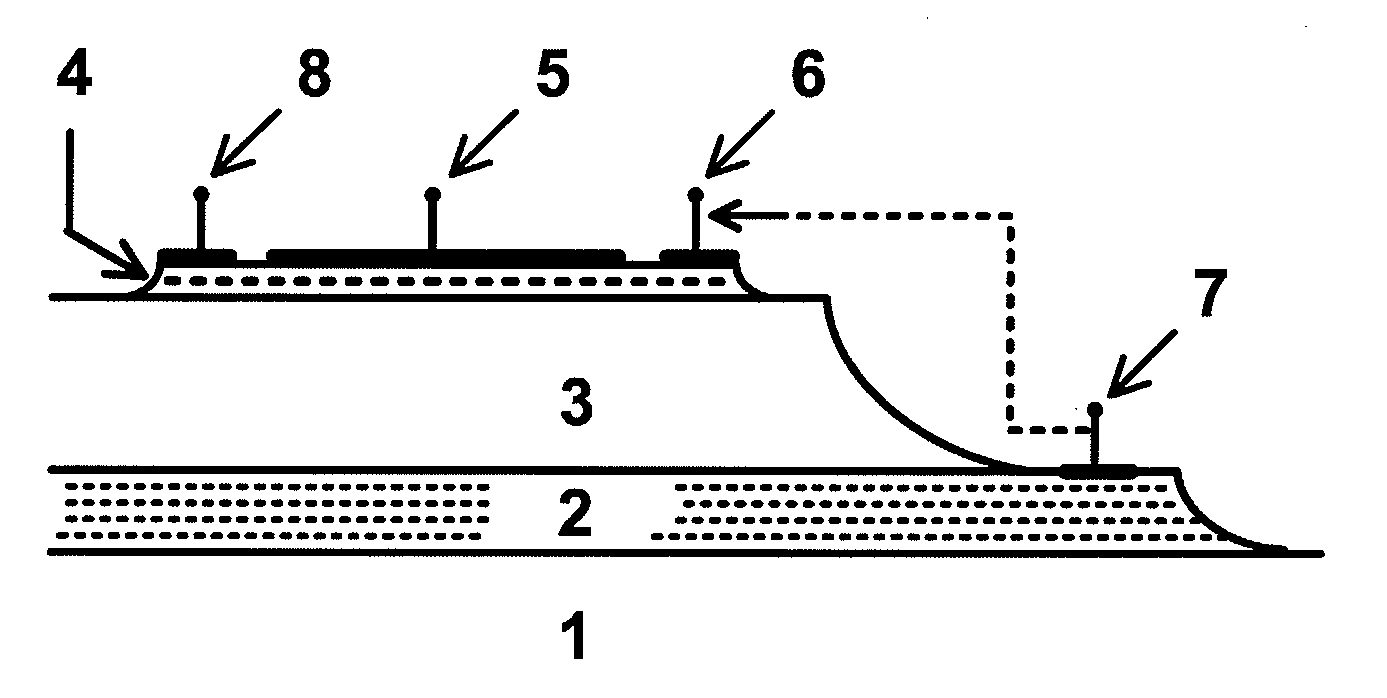
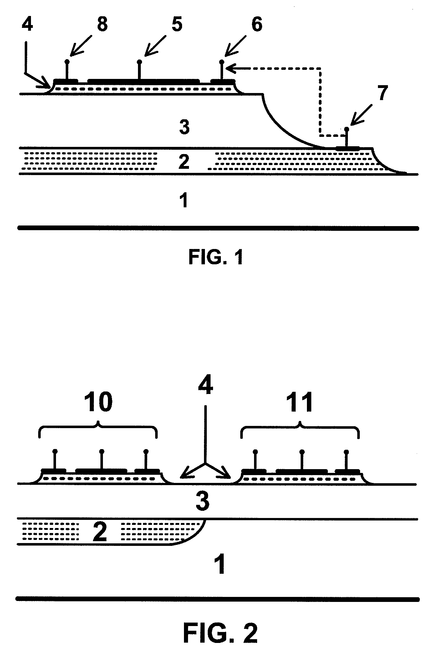
[0018]FIG. 2 shows an optimized application of the method of FIG. 1 for its use with semi-insulating GaAs substrates that allows to have regions with isolated devices with very good performances at high frequencies (11) and other regions (10) with very low excess noise devices protected by this invention, dedicated to local oscillator and mixing functions, all in the same monolithic integrated circuit (IC). The layer structure could be obtained easily starting from a semi-insulating GaAs substrate (1) where an initial p-type implantation or diffusion (2) would be done in those regions where the low excess noise resistors and transistors will be fabricated (note that a resistor has the same structure of the FET whose cross section appears in FIG. 1, if the gate terminal (5) is not fabricated and the Source (6) and Drain (8) terminals are used as the resistor's terminals). In this way we would obtain the screen-layers (2) under the low excess noise devices. The depth of said diffusion...

example 2

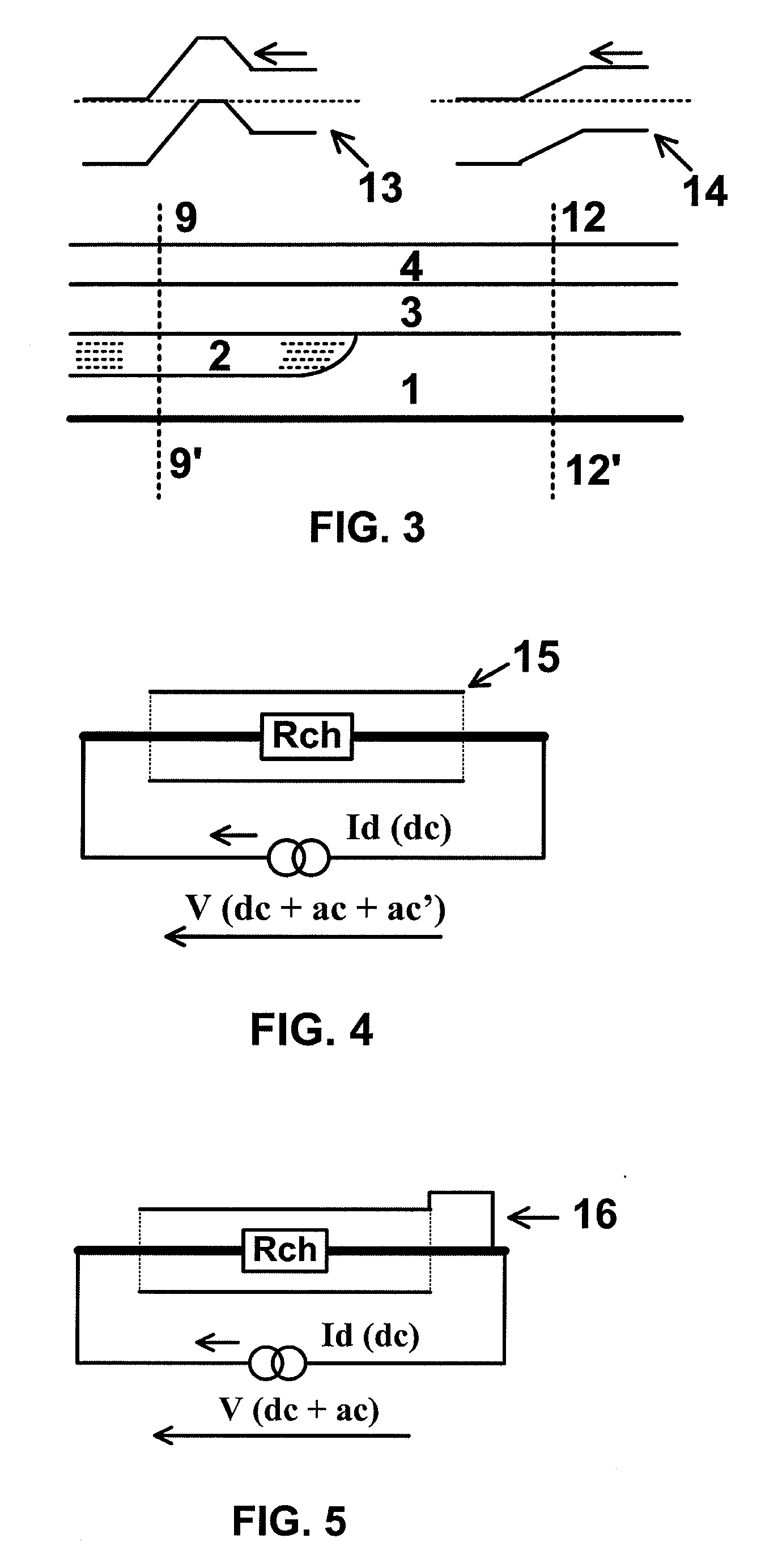
[0020]FIG. 4 shows the electrical cross section of many electrical devices having an inner conductive channel of a given resistance Rch surrounded by a neighbour conductor going in a roundabout way (14) to the former but isolated from it, that by Electrostatic laws forms a capacitor C surrounding the inner channel. The electrical geometry of FIG. 4 appears in many electronic devices going from a simple coaxial cable to a more sophisticated conducting filaments as the microwires and nanowires under active research today. From today's knowledge on excess noise, the resistance Rch of the inner channel when driven by the continuous (dc) current Id will allow to obtain a voltage V on the resistance Rch that will show a dc term given by Ohms Law: Vdc=Id×Rch and two small noise terms (ac) and (ac′), one being the thermal noise of the resistance Rch also known as Johnson noise and the second being a term not satisfactorily explained up to now that is the excess noise appearing for enough Id...


PUM


Abstract

This invention proposes the use of a thermodynamic screen placed under the electronic devices whose excess noise is to be reduced in order to block the transverse currents between said devices and subjacent layers that are responsible for the aforementioned excess noise. For epitaxial layers as those used in Microelectronics, the barrier layer (2) with an opposed doping to the epilayer supporting the devices (4), and the non-doped separating layer (3) form the thermodynamic screen which, embedded between the epilayer (4) and the substrate (1), reduces the aforementioned transverse currents and thus the excess noise of the devices on the epilayer (4) when they are biased. The connection between the ohmic contact (7) of the screen layer (2) with the source (6) of the FET transistors of the epilayer (4) (dashed line) or with their gate (5) removes the thermal noise of the capacitor that existed under those FET transistors and hence, the corresponding excess noise in these devices

Description

FIELD OF INVENTION[0001]The invention falls in the field of electrical devices and more specifically in the semiconductor-based devices widely used in microelectronics both as discrete as well as monolithically integrated devices. More specifically it pertains to the area of noise reduction techniques for low-frequency excess noise in devices.BACKGROUND OF THE INVENTION[0002]From the early observations of flicker noise in vacuum tubes in 1925, this kind of noise also found in solid-state devices and known as excess noise in resistors because it emerges over their thermal noise at low frequencies, always is found when a current flows in electrical devices. In regards to this noise, GaAs devices made on semi-insulating (SI) GaAs substrates are very noisy, thus being problematic for mixers due to noise upconversion effects that appears when the high level of noise at low frequencies of the mixing device (a MESFET for example) is translated to frequency bands where it degrades the syste...

Claims


Application Information

Patent Timeline
IPC IPC(8): H01L29/812
CPCH01L21/76H01L21/8252H01L27/0605H01L29/36H01L29/1075H01L29/1083H01L29/1087H01L29/10H01L21/2007H01L21/823857
Inventor IZPURA, JOSE IGNACIO
Owner UNIV MADRID POLITECNICA
Why Eureka
Try Eureka