Method for controlling delay time of pulse delay circuit and pulse delay circuit thereof

a technology of delay time and pulse delay, which is applied in the direction of pulse technique, instruments, horology, etc., can solve the problems of inability to meet the requirements of process technology alone, the circuit cannot be used for high-speed control purposes, and the manufacturing cost increases, so as to achieve the effect of reducing manufacturing costs, reducing manufacturing costs, and increasing the size of the circui

Active Publication Date: 2009-05-28
DENSO CORP
View PDF19 Cites 2 Cited by
  • Summary
  • Abstract
  • Description
  • Claims
  • Application Information

AI Technical Summary

Benefits of technology

[0048]In the time measurement circuit of the present invention, configured as described above, the control signal is supplied to the control terminal provided in the pulse delay circuit, via the control terminal, and the back gate voltage of the specific transistor configuring the delay unit is controlled. As a result, the range of available delay time is greater when the drive voltage is changed by the voltage setting circuit, compared to the conventional circuit. Therefore, a measurable time range can be widened without the size of the circuit being increased.

Problems solved by technology

In particular, when the measurement time Ta is extended, the circuit cannot be used for purposes requiring high-speed control.
Therefore, manufacturing costs increase.
Moreover, when a voltage resolution exceeding the capability of the process technology is required, such requirements cannot be met by reliance solely on the process technology.

Method used


Image

  • Method for controlling delay time of pulse delay circuit and pulse delay circuit thereof
  • Method for controlling delay time of pulse delay circuit and pulse delay circuit thereof
  • Method for controlling delay time of pulse delay circuit and pulse delay circuit thereof

Examples


first embodiment

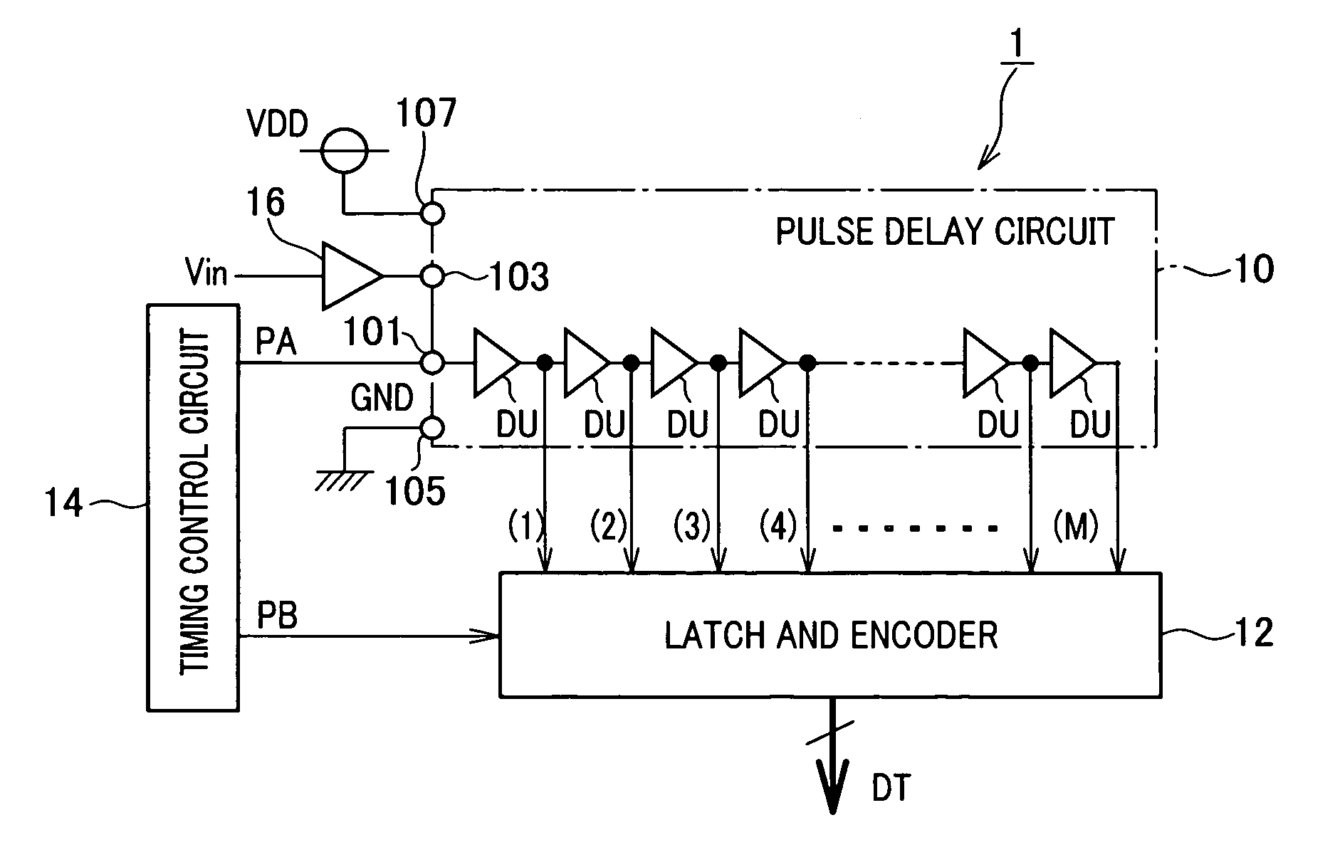
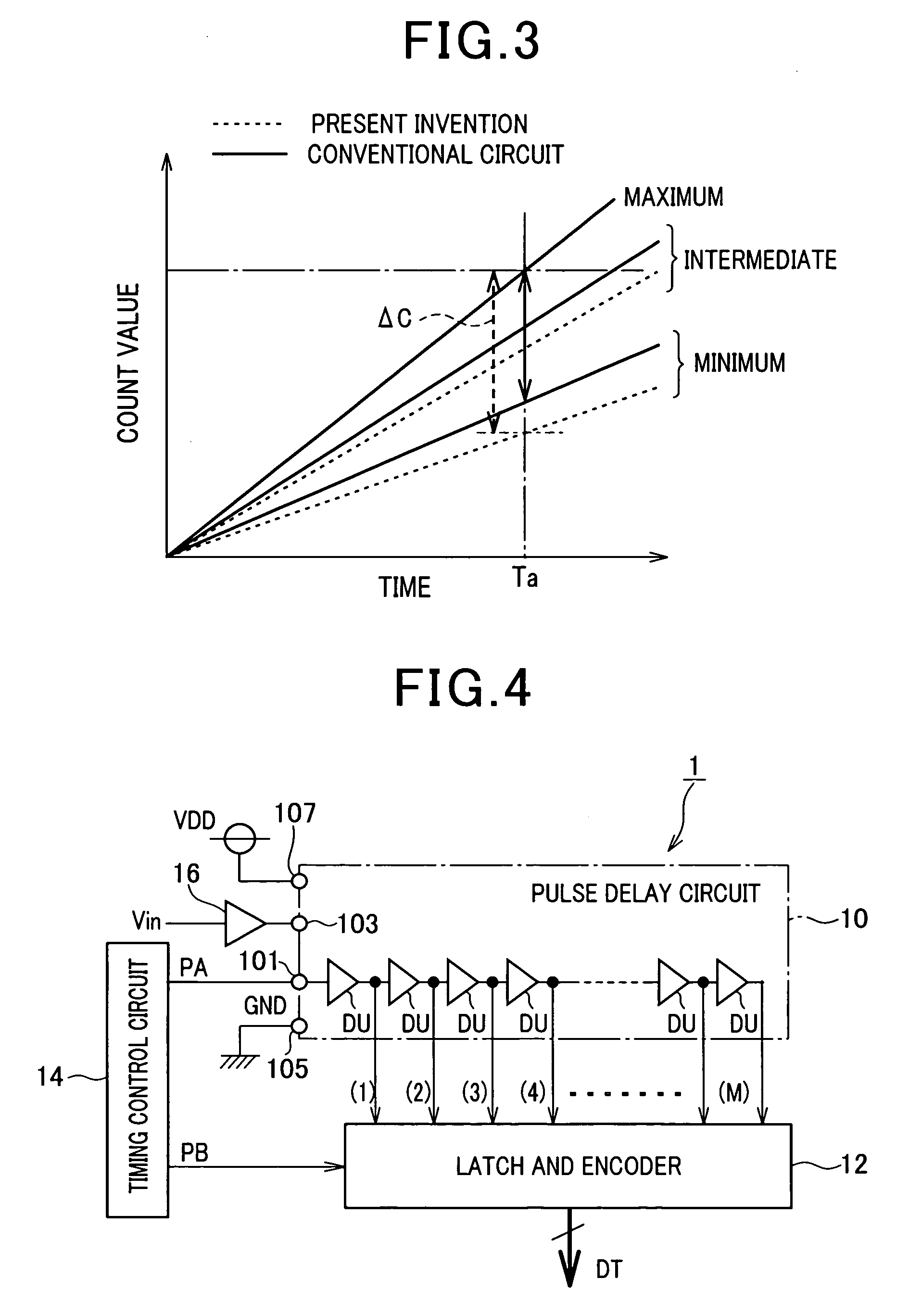
[0059]FIG. 4 is a block diagram showing an overall configuration of an A / D converter 1 to which the present invention is applied.

[0060]As shown in FIG. 4, the A / D converter 1 includes a pulse delay circuit 10, a latch and encoder 12, and a timing control circuit 14. The pulse delay circuit 10 is configured such that delay units DU are connected in a cascade configuration of M stages (M is a positive integer). A delay unit DU outputs a pulse signal PA after delaying the pulse signal PA by a predetermined delay time. The latch and encoder 12 serves as an encoding circuit that detects (latches) an arrival position of the pulse signal PA within the pulse delay circuit 10 at a rising timing of a sampling signal PB. The latch and encoder 12 then converts a detection result into digital data DT of a predetermined number of bits indicating the number of delay unit DU stages through which the pulse signal PA passed, and outputs the digital data DT as A / D conversion data. When an operation in...

second embodiment

[0074]Next, a second embodiment will be described.

[0075]FIG. 6 is a block diagram showing an overall configuration of an A / D converter 3 according to the second embodiment.

[0076]Only a portion of the configuration of the A / D converter 3 differs from that of the A / D converter 1 according to the first embodiment. Therefore, portions of the configuration that are the same are given the same reference numbers, and explanations thereof are omitted. The portion of the configuration that differs will mainly be described.

[0077]As shown in FIG. 6, the A / D converter 3 includes a control signal generation circuit 18. The control signal generation circuit 18 generates a control signal VC that is applied to the control terminal 107 based on an analog input signal Vin inputted via the buffer 16.

[0078]The control signal generation circuit 18 is configured to generate the control signal VC having a voltage level VDD+(VDD-Vin), with a maximum voltage of the analog input signal Vin serving as VDD. A ...

third embodiment

[0081]Next, a third embodiment will be described.

[0082]FIG. 7 is a block diagram showing an overall configuration of a time measurement circuit 5 to which the present invention is applied.

[0083]As shown in FIG. 7, the time measurement circuit 5 includes the pulse delay circuit 10, the latch and encoder 12, and a drive voltage setting circuit 20. The pulse delay circuit 10 and the latch and encoder 12 are configured in a manner similar to those configuring the A / D converter 1 according to the first embodiment. The drive voltage setting circuit 20 sets the drive voltage Vin applied to the positive drive terminal 103 of the pulse delay circuit 10.

[0084]The pulse signal PA supplied from an external source is applied to the pulse input terminal 101 of the pulse delay circuit 10. The negative drive terminal 105 is grounded. The fixed voltage VDD (Vmax=VDD=5V, according to the third embodiment) set to be the maximum voltage Vmax of the drive voltage Vin set by the drive voltage setting cir...


PUM


Abstract

An inverter circuit configuring a delay unit is a so-called CMOS transistor including a PMOS transistor and an NMOS transistor, of which respective gates are interconnected and respective drains are interconnected. The source and a back gate of the NMOS transistor are connected to the ground. The source of the PMOS transistor is connected to a positive drive terminal and controlled by an analog input signal. The back gate of the PMOS transistor is connected to a control terminal and controlled by a control signal.

Description

CROSS-REFERENCE TO RELATED APPLICATION[0001]This application is related to Japanese Patent Application No. 2007-307521 filed on Nov. 28, 2007, the contents of which are hereby incorporated by reference.BACKGROUND OF THE INVENTION[0002]1. Field of the Invention[0003]The present invention relates to a pulse delay circuit and a driving method thereof, and an analog-to-digital (A / D) conversion circuit and a time measurement circuit that use the pulse delay circuit. The pulse delay circuit includes delay units that delay signals, the delay units serially connected in a plurality of stages or connected to form a ring circuit.[0004]2. Description of the Related Art[0005]Conventionally, circuits that use a pulse delay circuit are known. The pulse delay circuit includes delay units serially connected in a plurality of stages or connected to form a ring circuit. A delay unit delays pulse signals by a delay time based on a voltage level of a drive signal. For example, as the circuits using the...

Claims


Application Information

Patent Timeline
Patent Type & Authority Applications(United States)
IPC IPC(8): H03M1/60H03H11/26G04F10/04H03K5/13H03M1/50
CPCH03K5/133
Inventor WATANABE, TAKAMOTOYAMAUCHI, SHIGENORI
Owner DENSO CORP
Why Eureka
Try Eureka