Air gap structure having protective metal silicide pads on a metal feature

a technology of air gap structure and metal feature, which is applied in the direction of semiconductor devices, semiconductor/solid-state device details, electrical apparatus, etc., can solve the problems of affecting the reliability characteristics of the interconnect structure, the overall speed of operation of the advanced semiconductor chip is approaching a limit, and the top surface of the exposed metal line is etch damaged

Active Publication Date: 2009-06-04
IBM CORP
View PDF12 Cites 36 Cited by
  • Summary
  • Abstract
  • Description
  • Claims
  • Application Information

AI Technical Summary

Benefits of technology

[0010]The present invention addresses the needs described above by providing an interconnect structure having a cavity in a low-k dielectric layer in which a metal feature adjoined to the cavity is protected by a metal silicide pad during an etch employed for formation of the cavity.

Problems solved by technology

With the progress in the semiconductor device technology leading to ultra large scale integration, the overall speed of operation of the advanced semiconductor chips is approaching a limit due to signal propagation delay in interconnection wires, which are employed as the high speed interconnect structures, between the individual semiconductor devices on the same advanced semiconductor chip.
An inevitable consequence of this prior art method is generation of etch damage to exposed top surfaces of a metal line during the isotropic etch.
Damages to the exposed top surfaces of the metal line by a reactive ion etch or a wet etch employing an etchant such as dilute hydrofluoric acid during the enlarging and merging of the cavities of a sublithographic diameter adversely impacts reliability characteristics of the interconnect structure.
High defect density, i.e., smaller grain size of the metal or high temperature typically increases electron scattering, and consequently, the amount of momentum transfer from the electrons to the conductor material.
Such momentum transfer, if performed sufficiently cumulatively, may cause the metal ions to dislodge from the lattice and move physically.
Thus, presence of physical defects, as is generated in the prior art interconnect structure of Edelstein et al., thus increases electron scattering during conduction of current, and degrades electromigration resistance of the metal line.
Reliability of the prior art interconnect structure is undermined since formation of voids through electromigration is accelerated due to the presence of the defects formed on surfaces of a metal line during the merging of the sublithographic cavities.

Method used


Image

  • Air gap structure having protective metal silicide pads on a metal feature
  • Air gap structure having protective metal silicide pads on a metal feature
  • Air gap structure having protective metal silicide pads on a metal feature

Examples


Embodiment Construction

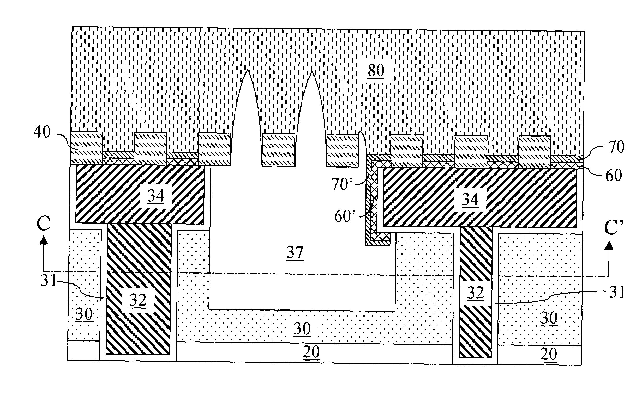
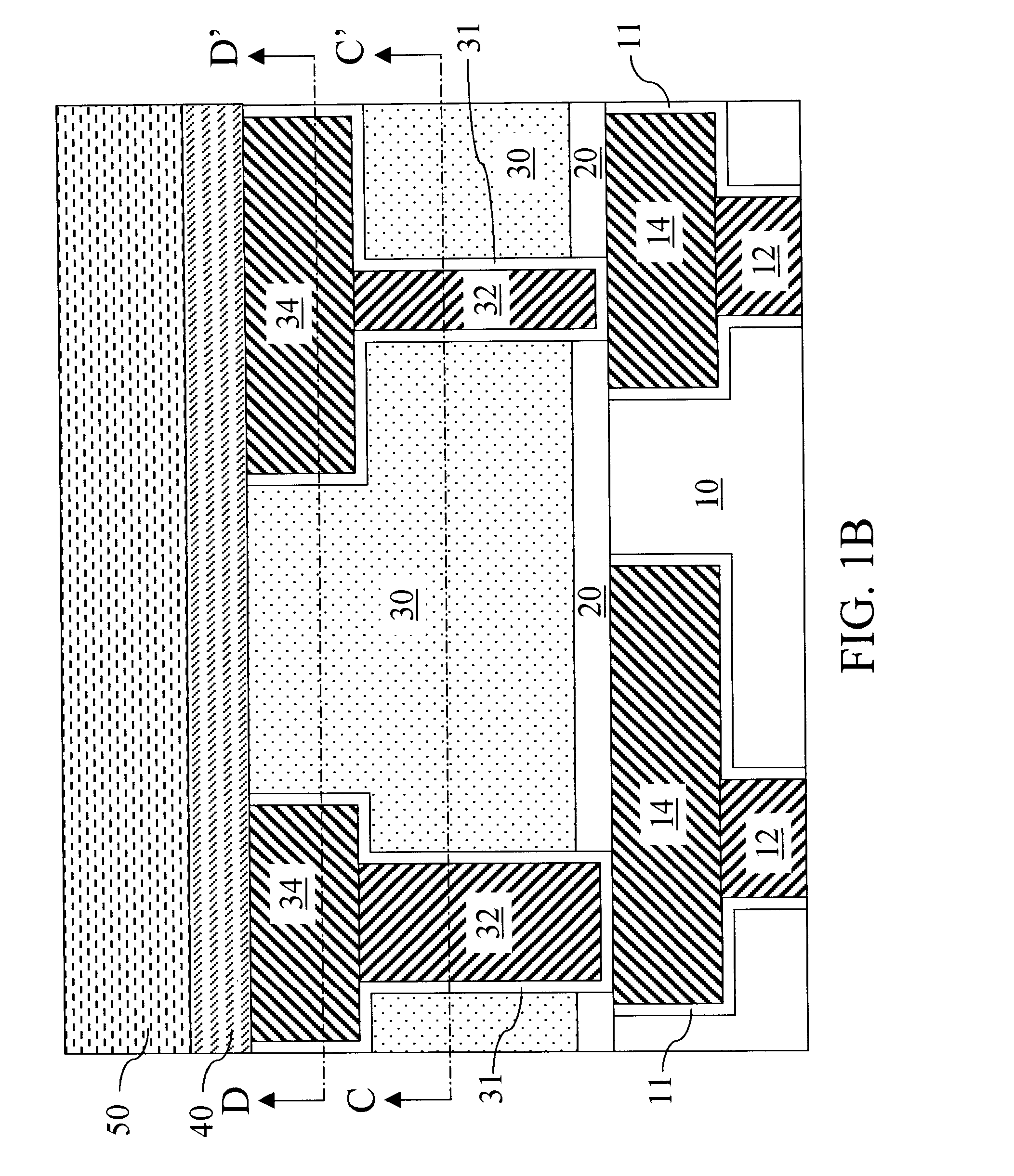
[0068]As stated above, the present invention relates to an interconnect structure having protective metal silicide pads on a metal feature and methods of manufacturing the same, which are now described in detail with accompanying figures. It is noted that like and corresponding elements mentioned herein and illustrated in the drawings are referred to by like reference numerals.

[0069]Referring to FIGS. 1A-1D, an exemplary interconnect structure according to the present invention is shown, which comprises a metal feature, which is at least one metal line 34. The exemplary interconnect structure further comprises at least one metal via 32, and at least one metallic liner 31 that are embedded in a low dielectric constant (low-k) material layer 30 that comprise a low-k dielectric material having a dielectric constant less than 2.8. The exemplary interconnect structure further comprises at least one underlying metal line 14, at least one underlying metal via 12, and at least one underlyin...


PUM

PropertyMeasurementUnit
dielectric constantaaaaaaaaaa
diameteraaaaaaaaaa
thicknessaaaaaaaaaa

Abstract

A hard mask is formed on an interconnect structure comprising a low-k material layer and a metal feature embedded therein. A block polymer is applied to the hard mask layer, self-assembled, and patterned to form a polymeric matrix of a polymeric block component and containing cylindrical holes. The hard mask and the low-k material layer therebelow are etched to form cavities. A conductive material is plated on exposed metallic surfaces including portions of top surfaces of the metal feature to form metal pads. Metal silicide pads are formed by exposure of the metal pads to a silicon containing gas. An etch is performed to enlarge and merge the cavities in the low-k material layer. The metal feature is protected from the etch by the metal silicide pads. An interconnect structure having an air gap and free of defects to surfaces of the metal feature is formed.

Description

FIELD OF THE INVENTION [0001]The present invention relates to semiconductor structures, and particularly to an interconnect structure having protective metal silicide pads on a metal feature and methods of manufacturing the same.BACKGROUND OF THE INVENTION[0002]Advanced semiconductor chips, such as high performance microprocessor, microcontroller and communication chips, require high speed interconnect structures between individual semiconductor devices which are used to perform various functions such as logical operations, storing and retrieving data, providing control signals and the like. With the progress in the semiconductor device technology leading to ultra large scale integration, the overall speed of operation of the advanced semiconductor chips is approaching a limit due to signal propagation delay in interconnection wires, which are employed as the high speed interconnect structures, between the individual semiconductor devices on the same advanced semiconductor chip.[000...

Claims


Application Information

Patent Timeline
Patent Type & Authority Applications(United States)
IPC IPC(8): H01L23/52H01L21/4763
CPCH01L21/31144H01L21/7682H01L21/76849H01L21/76852H01L23/5222H01L2924/0002H01L23/53238H01L23/53295H01L2924/00
Inventor BONILLA, GRISELDAEDELSTEIN, DANIEL C.NITTA, SATYANARAYANA V.NOGAMI, TAKESHIPONOTH, SHOMRATH, DAVID L.YANG, CHIH-CHAO
Owner IBM CORP
Why Eureka
Try Eureka