

Current-perpendicular-to-the-plane structure magnetoresistive element and method of making the same and storage apparatus
a technology of magnetoresistive elements and which is applied in the field of current perpendicular to the plane (cpp) structure magnetoresistive elements, can solve problems such as deterioration of detection sensitivity, and achieve the effect of high accuracy
- Summary
- Abstract
- Description
- Claims
- Application Information
AI Technical Summary
Benefits of technology
Problems solved by technology
Method used
Image

Examples
first embodiment
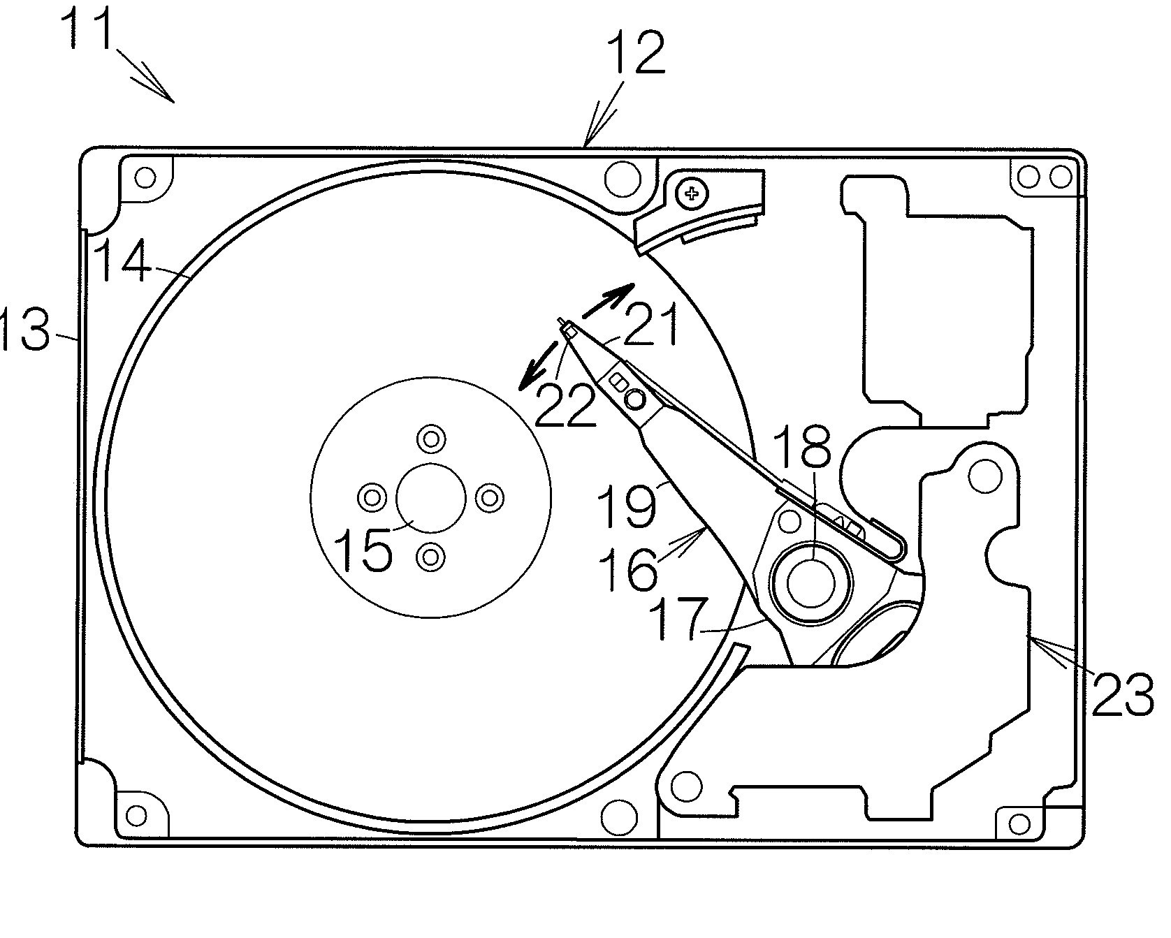
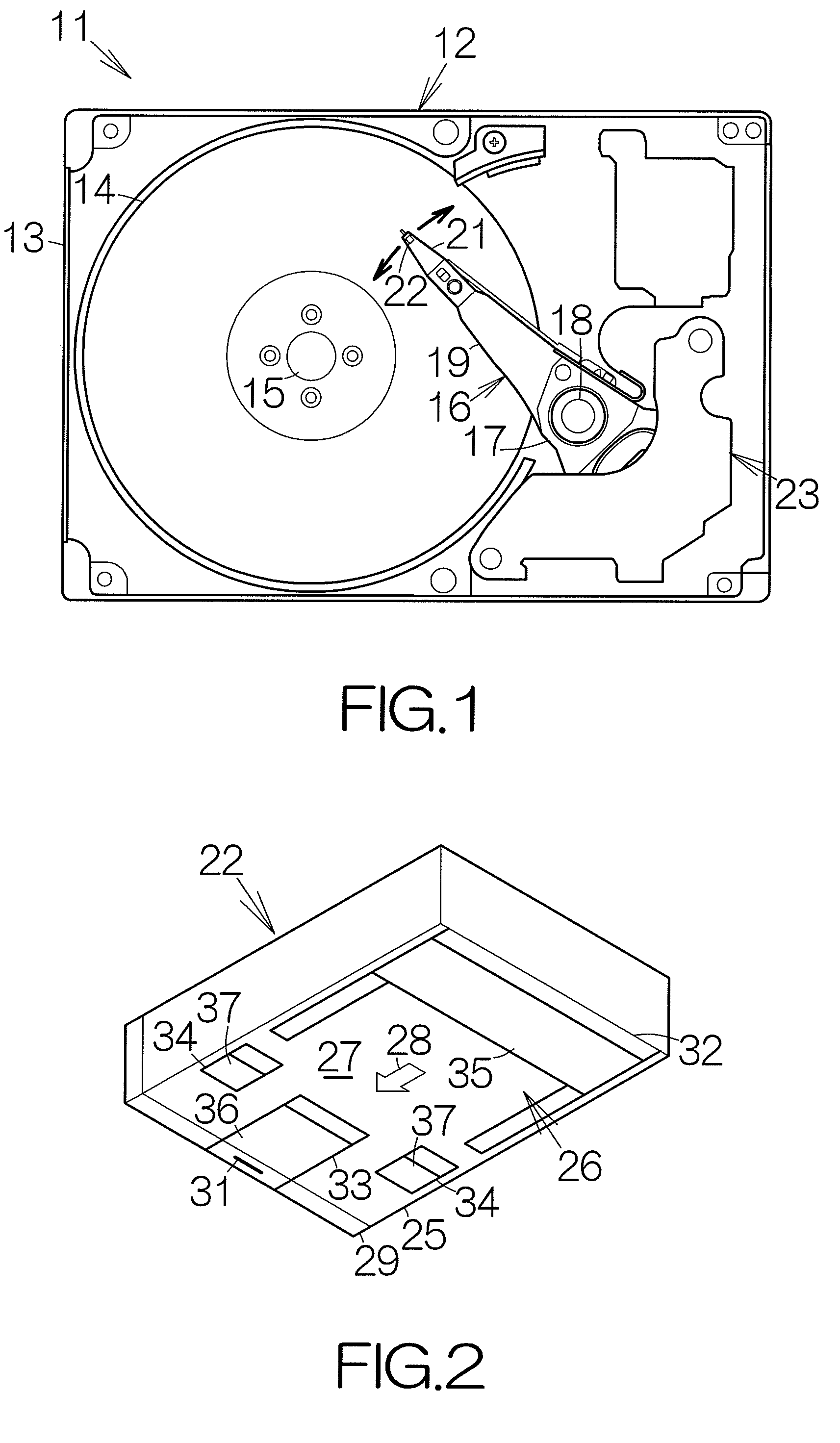
[0037]FIG. 1 schematically illustrates the inner structure of a hard disk drive, HDD, 11 as an example of a storage medium drive or storage apparatus according to the present invention. The hard disk drive 11 includes an enclosure 12. The enclosure 12 includes an enclosure cover, not shown, and a box-shaped enclosure base 13 defining an inner space of a flat parallelepiped, for example. The enclosure base 13 may be made of a metallic material such as aluminum, for example. Molding process may be employed to form the enclosure base 13. The enclosure cover is coupled to the enclosure base 13. The enclosure cover closes the opening of the enclosure base 13. Pressing process may be employed to form the enclosure cover out of a plate material, for example.
[0038]At least one magnetic recording disk 14 as a storage medium is placed in the inner space of the enclosure base 13. The magnetic recording disk or disks 14 are mounted on the driving shaft of a spindle motor 15. The spindle motor 1...
second embodiment
[0094]FIG. 19 schematically illustrates the structure of a magnetoresistive random access memory (MRAM) 81 as a storage apparatus according to a The MRAM 81 includes memory cells 82 arranged in a matrix, for example. The individual memory cell 82 includes a metal oxide semiconductor field-effect transistor (MOSFET) 83. The MOSFET 83 is either a p-type MOSFET or an n-type MOSFET. Here, the MOSFET 83 is a p-type MOSFET.
[0095]The MOSFET 83 includes a base member, namely a silicon substrate 84. The silicon substrate 84 defines a p-well region 85 containing a p-type impurity. A pair of impurity diffusion regions 86a, 86b are defined on the p-well region 85 at positions distanced from each other. N-type impurity is introduced into the impurity diffusion regions 86a, 86b. The impurity diffusion region 86a provides a source region S. The impurity diffusion region 86b provides a drain region D. A gate insulating layer 87 is formed on the surface of the silicon substrate 84 at a position bet...
PUM
| Property | Measurement | Unit |
|---|---|---|
| thickness | aaaaa | aaaaa |
| thickness | aaaaa | aaaaa |
| thickness | aaaaa | aaaaa |
Abstract
Description
Claims
Application Information