
Manufacturing method of semiconductor device

Inactive Publication Date: 2009-06-04
SEMICON ENERGY LAB CO LTD
View PDF5 Cites 75 Cited by
  • Summary
  • Abstract
  • Description
  • Claims
  • Application Information

AI Technical Summary

Benefits of technology

[0010]Accordingly, an object is to manufacture a semiconductor device which has higher integration and thus is reduced in thickness and size. In addition, another object is to achieve higher performance and lower electric power consumption in the semiconductor device.
[0034]In addition, since the semiconductor element layers manufactured over the different substrates through different processes are stacked for integration, the semiconductor element layers each having excellent characteristics can be formed in an optimized condition (a material, thickness, and an element structure) without being influenced by manufacturing conditions of the semiconductor element layer in a different layer. Accordingly, a semiconductor device with a multi-layer structure with a plurality of semiconductor elements can also have higher performance.

Problems solved by technology

However, as described above, if an adhesive layer such as an interlayer insulator of an organic material or a resin is formed between semiconductor element layers, a semiconductor device becomes thick and large.
Moreover, a problem that electrical connection between the semiconductor element layers is difficult is also concerned.

Method used


Image

  • Manufacturing method of semiconductor device
  • Manufacturing method of semiconductor device
  • Manufacturing method of semiconductor device

Examples


embodiment mode 1

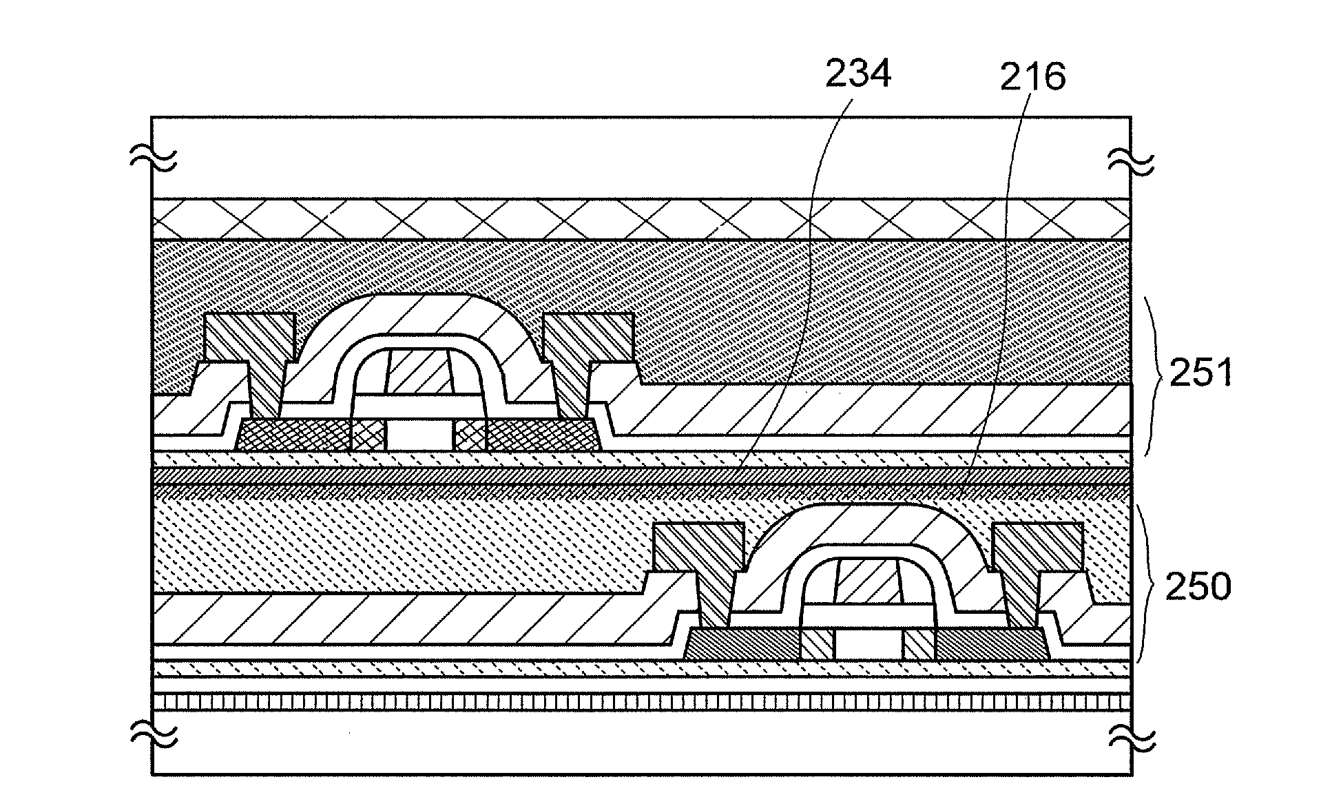
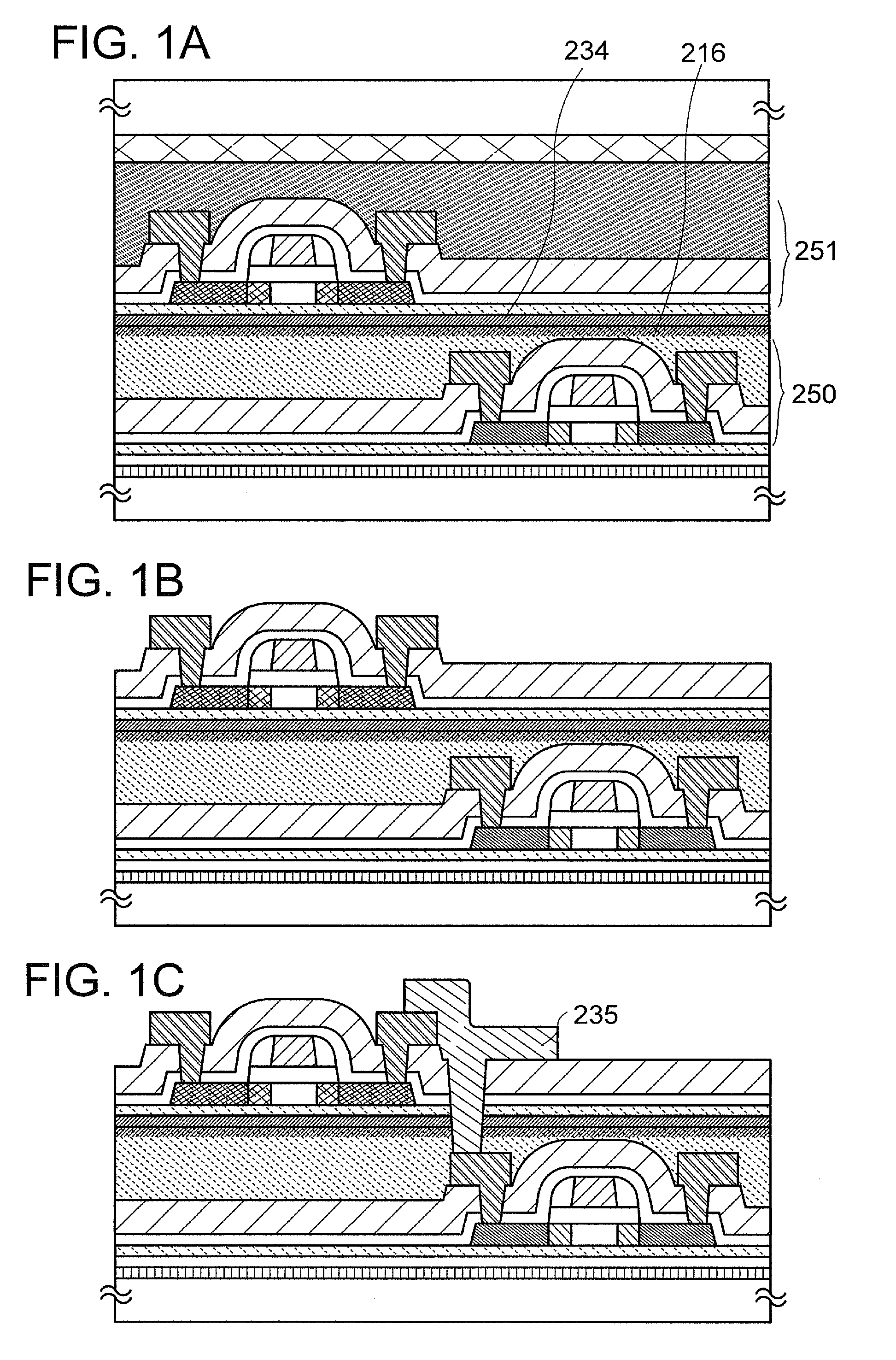
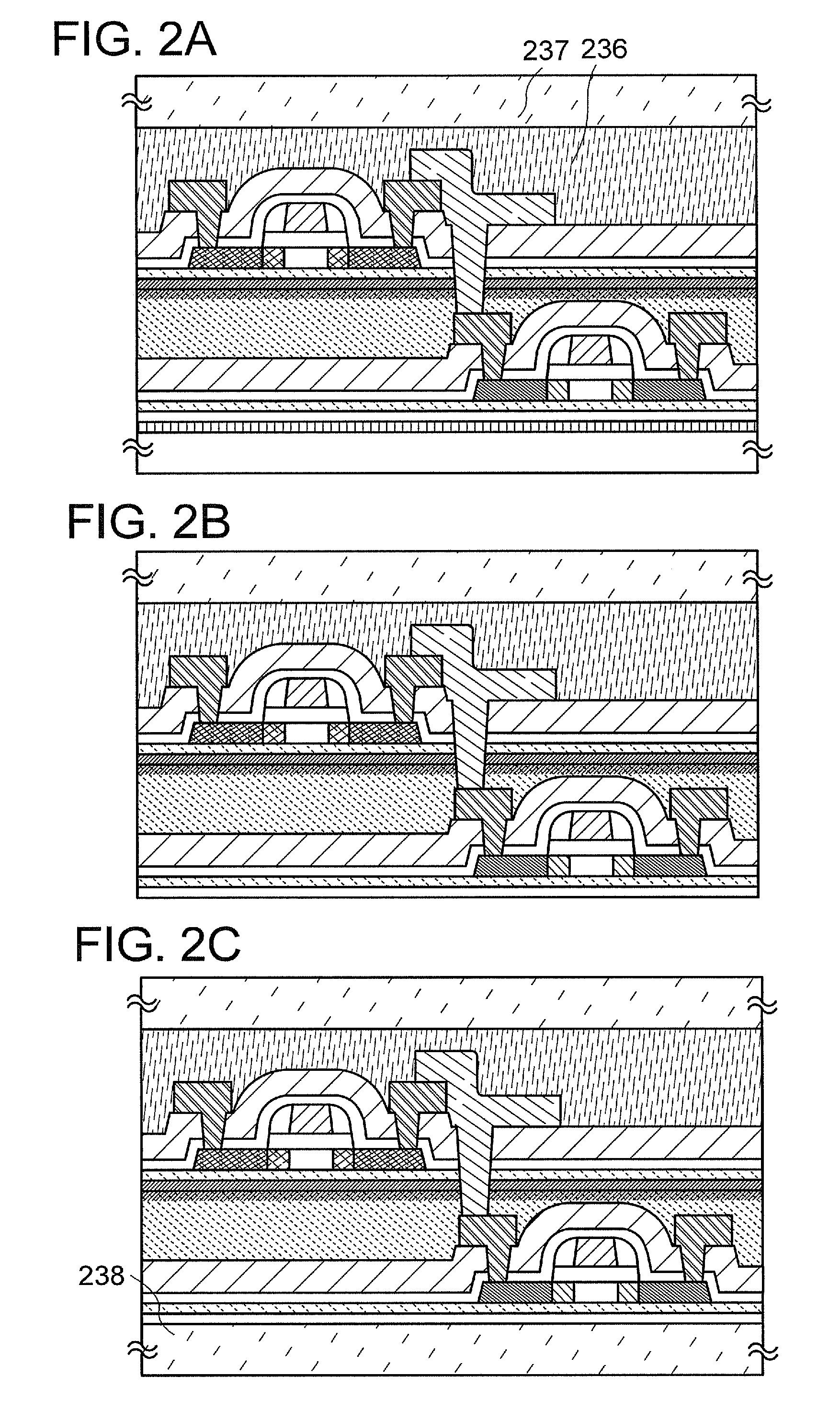
[0063]In this embodiment mode, a semiconductor device aimed at increase in integration and reduction in thickness and size, and a manufacturing method of the semiconductor device will be described in detail with reference to FIGS. 1A to 1C, FIGS. 2A to 2C, FIGS. 3A to 3D, FIGS. 4A to 4E, and FIGS. 10A and 10B.

[0064]In this embodiment mode, as an example of a semiconductor device, a CMOS (complementary metal oxide semiconductor) will be described.

[0065]A semiconductor device of this embodiment mode has a multi-layer structure in which semiconductor element layers are stacked. The semiconductor element layer is separated from a substrate used when the semiconductor element layer is formed, and stacked over another semiconductor element layer by bonding between insulating layers. Note that in this specification, a substrate over which the semiconductor element layer is formed is also referred to as a formation substrate. Accordingly, the semiconductor element layer is formed over the f...

embodiment mode 2

[0199]In this embodiment mode, a different example of steps for bonding a single crystal semiconductor layer from a single crystal semiconductor substrate to a formation substrate in Embodiment Mode 1 will be described with reference to FIGS. 19A to 19E. Therefore, repeated descriptions for the same components as or components having similar functions to the components in Embodiment Mode 1 are omitted.

[0200]The single crystal semiconductor substrate 1108 shown in FIG. 19A is purified and ions accelerated by an electric field is added at a predetermined depth from its surface, thereby forming the weakened layer 1110.

[0201]Next, the inorganic insulating film 1109 is formed over the single crystal semiconductor substrate 1108 in which the weakened layer 1110 is provided, and the separation layer 1130 is formed over the inorganic insulating film 1109 (see FIG. 19B). In this manner, the separation layer may be provided on the single crystal semiconductor side. In other words, the separat...

embodiment mode 3

[0208]In this embodiment mode, a different example of steps for bonding a single crystal semiconductor layer from a single crystal semiconductor substrate to a formation substrate in Embodiment Mode 1 will be described. Therefore, repeated descriptions for the same components as or components having similar functions to the components in Embodiment Mode 1 are omitted.

[0209]In this embodiment mode, when single crystal semiconductor layers are transferred from a single crystal semiconductor substrate, the single crystal semiconductor substrate is etched selectively (this step is also referred to as groove processing), and a plurality of single crystal semiconductor layers divided such that they have the size of semiconductor elements to be manufactured are transferred to a formation substrate. Thus, a plurality of island-shaped single crystal semiconductor layers can be formed over the formation substrate. Since the single crystal semiconductor layers which are processed into an eleme...


PUM


Abstract

A semiconductor device which has higher integration and is further reduced in thickness and size. A semiconductor device with high performance and low power consumption. A semiconductor element layer separated from a substrate by using a separation layer is stacked over a semiconductor element layer formed by using another substrate and covered with a flattened inorganic insulating layer. After separation of the semiconductor element layer in a top layer from the substrate, the separation layer is removed so that an inorganic insulating film formed under the semiconductor element layer is exposed. The flattened inorganic insulating layer and the inorganic insulating film are made to be in close contact and bonded to each other. In addition, a semiconductor layer included in the semiconductor element layer is a single crystal semiconductor layer which is separated from a semiconductor substrate and transferred to a formation substrate.

Description

BACKGROUND OF THE INVENTION[0001]1. Field of the Invention[0002]This invention relates to a method of manufacturing a semiconductor device having a multi-layer structure.[0003]2. Description of the Related Art[0004]In a technical field of semiconductor devices, higher performance and lower electric power consumption have been promoted by miniaturization and higher integration. In order to increase the integration of semiconductor integrated circuits, a multi-layer integrated circuits with integrated circuits (semiconductor element layer) of a multi-layer structure have been proposed.[0005]As an example of manufacturing such a multi-layer integrated circuit, a method in which an interlayer insulator of an organic material is formed over a first semiconductor element layer which is formed over a substrate, and a second semiconductor element layer is stacked over the interlayer insulator has been disclosed (for example, see Patent Document 1: Japanese Published Patent Application No. H...

Claims


Application Information

Patent Timeline
IPC IPC(8): H01L21/76H01L21/84H01L21/02
CPCH01L21/8221H01L27/0688H01L27/13H01L27/1266H01L27/1214H01L2224/80896H01L2224/9202H01L2224/9212H01L2224/8203H01L2224/821H01L2224/80001H01L2224/82
Inventor TSUCHIYA, KAORU
Owner SEMICON ENERGY LAB CO LTD
Features
  • Generate Ideas
  • Intellectual Property
  • Life Sciences
  • Materials
  • Tech Scout
  • Unparalleled Data Quality
  • Higher Quality Content
  • 60% Fewer Hallucinations
Learn More