Eureka AIR delivers breakthrough ideas for toughest innovation challenges, trusted by R&D personnel around the world.

Method of forming a modified layer in a substrate

a technology of modified layers and substrates, applied in the direction of manufacturing tools, metal working equipment, welding/soldering/cutting articles, etc., can solve the problems of substrate splitting, device subject to division, and high risk of chipping, so as to prevent the strength of the substrate from being reduced, the strength of the substrate can be maintained, and the strength of the substrate can be reduced.

Active Publication Date: 2009-06-11
DISCO CORP
View PDF6 Cites 11 Cited by
  • Summary
  • Abstract
  • Description
  • Claims
  • Application Information

AI Technical Summary

Benefits of technology

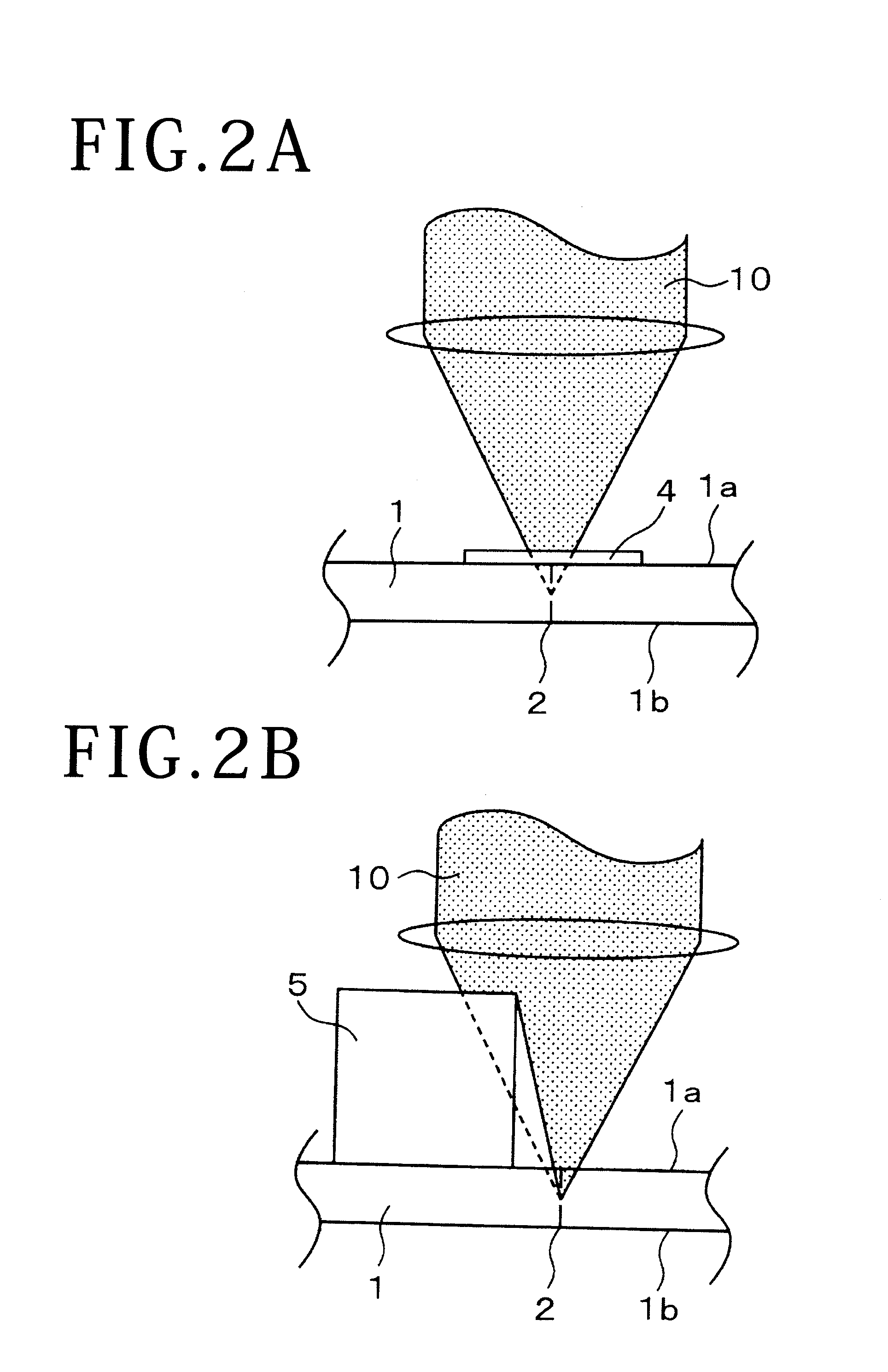
[0007]Accordingly, it is an object of the invention to provide a method of reliably forming a modified-layer inside a substrate with a laser beam even if the substrate is stacked with a stacked article on an optical path of the laser beam when the modified layer is formed inside the substrate by directing the laser beam to the substrate along a predetermined dividing line.
[0009]In the method of forming a modified layer in a substrate according to the present invention, before the stacked articles are stacked on the substrate, the modified layer is previously formed inside the substrate by irradiation of the laser beam. Thus, the modified layer is formed over the entire areas of the entire predetermined dividing lines. As a result, while production of chippings is prevented, the substrate can be split along the predetermined dividing lines.
[0012]Incidentally, the substrate lowers in strength in proportion to the length of the predetermined dividing lines formed with the modified layers. In other words, the shorter the predetermined dividing lines formed with the modified layers, the more the strength of the substrate can be maintained after the formation of the modified layers. In the present invention, the modified layer is formed only at the interrupted area as a required minimum area in the first modified-layer forming step; therefore, the strength of the substrate can be prevented from being reduced. As a result, even after the first modified-layer forming step, handling liable to apply external force to the substrate or stacking work of a stacked article can be smoothly carried out. In addition, it is not necessary to direct the laser beam from the rear surface of the substrate; therefore, even the substrate stacked with the stacked articles on the front surface and formed with the metal film on the rear surface can be formed with the modified layers over the entire areas of all the predetermined dividing lines.
[0013]According to the present invention, even the substrate stacked with the stacked articles on the predetermined dividing lines can reliably be formed with the modified layers inside the substrate along all the predetermined dividing lines. This can provide an effect of preventing production of chippings and of splitting the substrate along the predetermined dividing lines upon application of external force to the substrate. In addition, the modified layer is formed only at the interrupted area in the first modified-layer forming step and the modified layer is formed along the remaining predetermined dividing lines in the second modified-layer forming step; therefore, the strength of the substrate can be maintained after the first modified-layer forming step. This provides an effect that handling or stacking work of a stacking article can smoothly be carried out and the modified layers can be formed along all the predetermined dividing lines.

Problems solved by technology

If external force is applied to the substrate in such a condition, since an area formed with no modified-layer is present inside the substrate, a device subjected to the division may be likely to produce chippings, i.e., cracks or burrs.
In addition, a problem may occur in that the substrate is split while largely deviating from a predetermined dividing line.

Method used


Image

  • Method of forming a modified layer in a substrate
  • Method of forming a modified layer in a substrate
  • Method of forming a modified layer in a substrate

Examples


Embodiment Construction

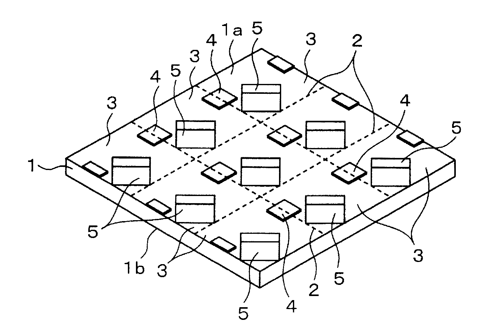
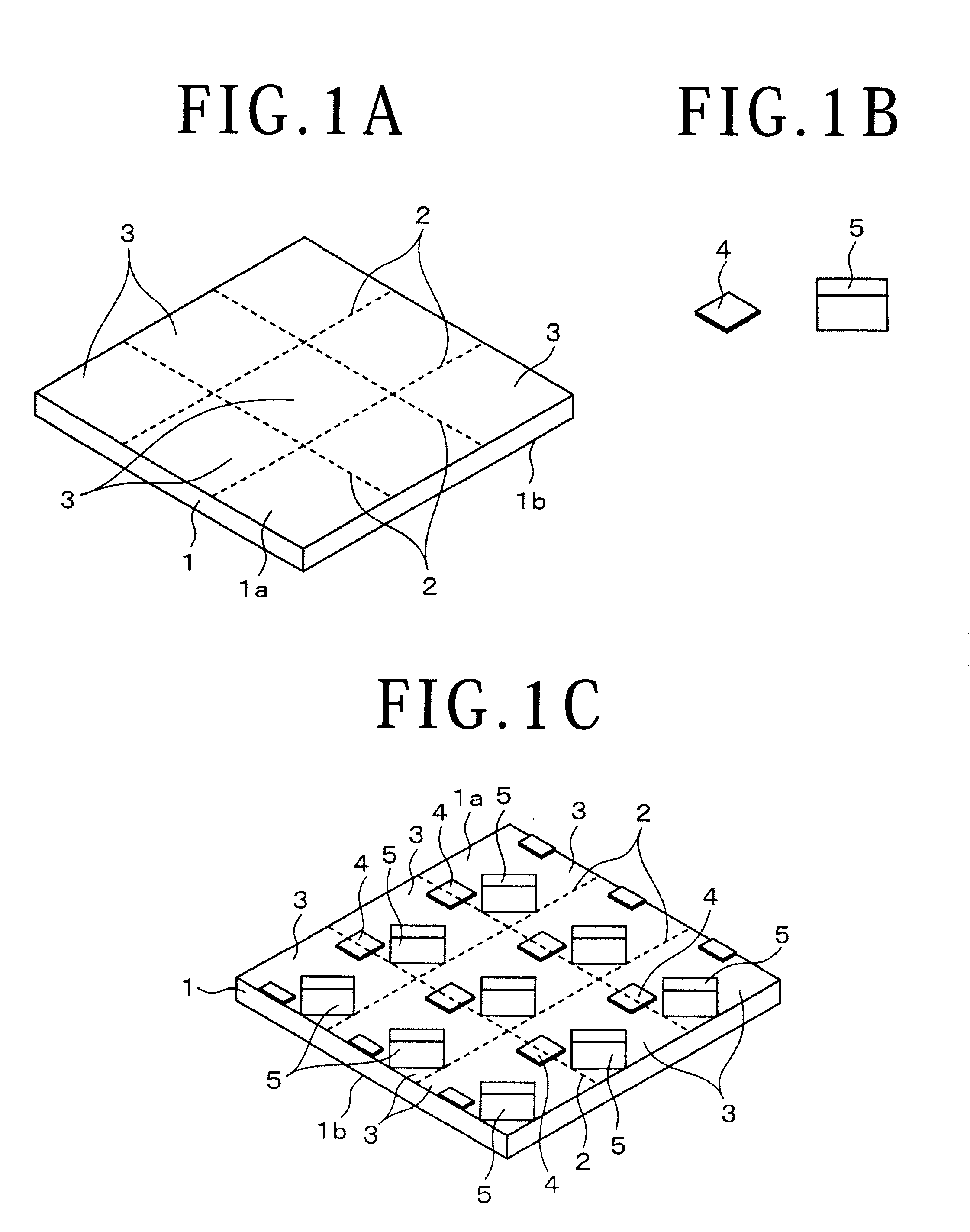
[0023]A preferred embodiment of the present invention will hereinafter be described with reference to the drawings. Reference numeral 1 of FIG. 1A denotes a substrate to be formed with a modified layer by a modified-layer forming method according the embodiment. This substrate 1 is a silicon wafer or the like. A plurality of rectangular device areas 3 are sectioned on a front surface 1a of the substrate 1 along lattice-like predetermined dividing lines 2. Stacked articles 4, 5 such as TEGs, elements and the like shown in FIG. 1B are stacked in these device areas 3. These stacked articles 4, 5 are formed of a material such as metal absorbing or reflecting a laser beam. FIG. 1C illustrates the substrate 1 (the assembly) stacked with the stacked articles 4, 5 on the front surface 1a. The stacked article 4 is stacked to cover the predetermined dividing line 2 and to be spanned between adjacent device areas 3. The stacked article 4 is cut along the corresponding dividing line 2 concurren...


PUM

PropertyMeasurementUnit
areaaaaaaaaaaa
external forceaaaaaaaaaa
areasaaaaaaaaaa

Abstract

First, mapping data storing interrupted areas is obtained. In a first modified-layer forming step, before a stacked article is stacked on a front surface of a substrate, a laser beam is directed to the interrupted areas based on the mapping data to form modified layers only at the interrupted areas. After the stacked articles have been stacked on the substrate, in a second modified-layer forming step, the laser beam is directed at least to the predetermined dividing line formed with no modified layer in the first modified-layer forming step to form a modified layer.

Description

BACKGROUND OF THE INVENTION[0001]1. Field of the Invention[0002]The present invention relates to a modified-layer forming method of forming a modified layer inside a substrate by directing a laser beam to the substrate such as a semiconductor wafer or the like.[0003]2. Description of the Related Art[0004]A substrate such as a semiconductor wafer is sectioned by predetermined dividing lines into device areas to be formed with devices thereon. After the devices are formed in the device areas, the substrate is subjected to steping such as polishing. The substrate is cut along the predetermined dividing lines to provide the devices (semiconductor chips). Various methods are adopted as substrate cutting methods, including a method of using a cutting blade, and a method of cutting a wafer by directing a laser beam to the wafer to form slits therein by a thermal transpiration phenomenon called ablation.[0005]One of the substrate cutting methods described above is a method of dividing a sub...

Claims


Application Information

Patent Timeline
Patent Type & Authority Applications(United States)
IPC IPC(8): H01L21/268B23K26/00B23K26/064B23K101/40H01L21/301
CPCB23K26/0057B23K26/4075H01L21/78B28D5/0011B23K2201/40B23K26/40B23K26/53B23K2101/40B23K2103/50
Inventor WATANABE, YOSUKEFURUTA, KENJIOHSUGA, KIYOSHI
Owner DISCO CORP
Why Eureka
Eureka Blog
Learn More