Semiconductor device

a technology of semiconductor devices and semiconductors, applied in semiconductor devices, semiconductor/solid-state device details, diodes, etc., can solve the problems of metal portion on polycrystalline silicon susceptible to fluctuations and receive effects, and achieve the effect of small resistance variation and less likely to fluctua

Active Publication Date: 2009-06-18
ABLIC INC
View PDF2 Cites 6 Cited by
  • Summary
  • Abstract
  • Description
  • Claims
  • Application Information

AI Technical Summary

Benefits of technology

[0017]According to the present invention, it is possible to provide a semiconductor device including a resistor circuit formed of polycrystalline silicon resistors which are less likely to fluctuate due to the influence of the semiconductor manufacturing steps and which are stable because of small resistance variation.

Problems solved by technology

The conventional method of stabilizing the resistance of the polycrystalline silicon as described above has, however, the following problem.
Specifically, the metal portion on the polycrystalline silicon is susceptible and receives effects caused by, for example, heat, stress, and charge due to plasma, other than hydrogen which affect the polycrystalline silicon in the semiconductor manufacturing process.

Method used


Image

  • Semiconductor device
  • Semiconductor device
  • Semiconductor device

Examples


first embodiment

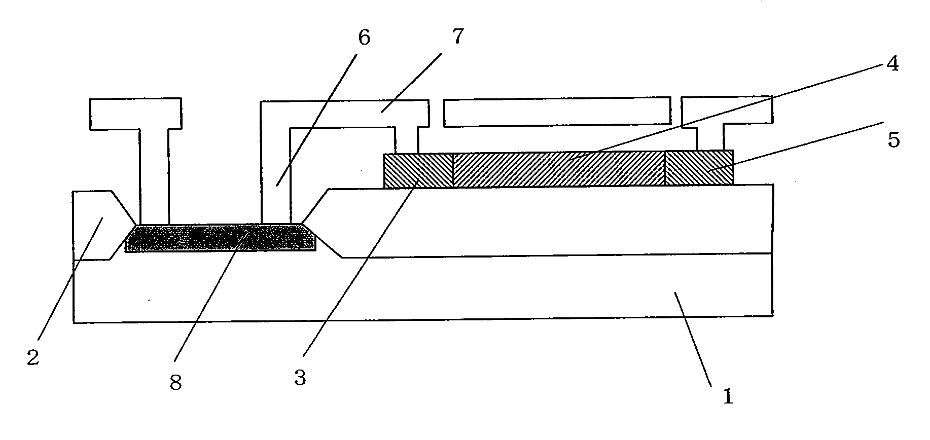
[0032]FIG. 4 is a cross-sectional view of a main portion illustrating the present invention for realizing the resistor circuit of FIG. 3. In this embodiment, an interconnecting layer which serves to connect a resistor and a metal line is formed of an impurity diffusion layer formed in a semiconductor substrate. The impurity diffusion layer is configured so that impurities having a polarity opposite to a polarity of the semiconductor substrate are selected, and a leak current does not flow excessively in the semiconductor substrate 1 when voltage is applied to the resistor circuit. Further, an impurity implantation dose is selected according to voltage applied to the resistor circuit so that a diode including the semiconductor substrate 1 and the impurity diffusion layer does not cause junction failure due to the voltage application.

[0033]The advantage of using the impurity diffusion layer formed in the semiconductor substrate 1 as the interconnecting layer 8 in this embodiment is a ...

second embodiment

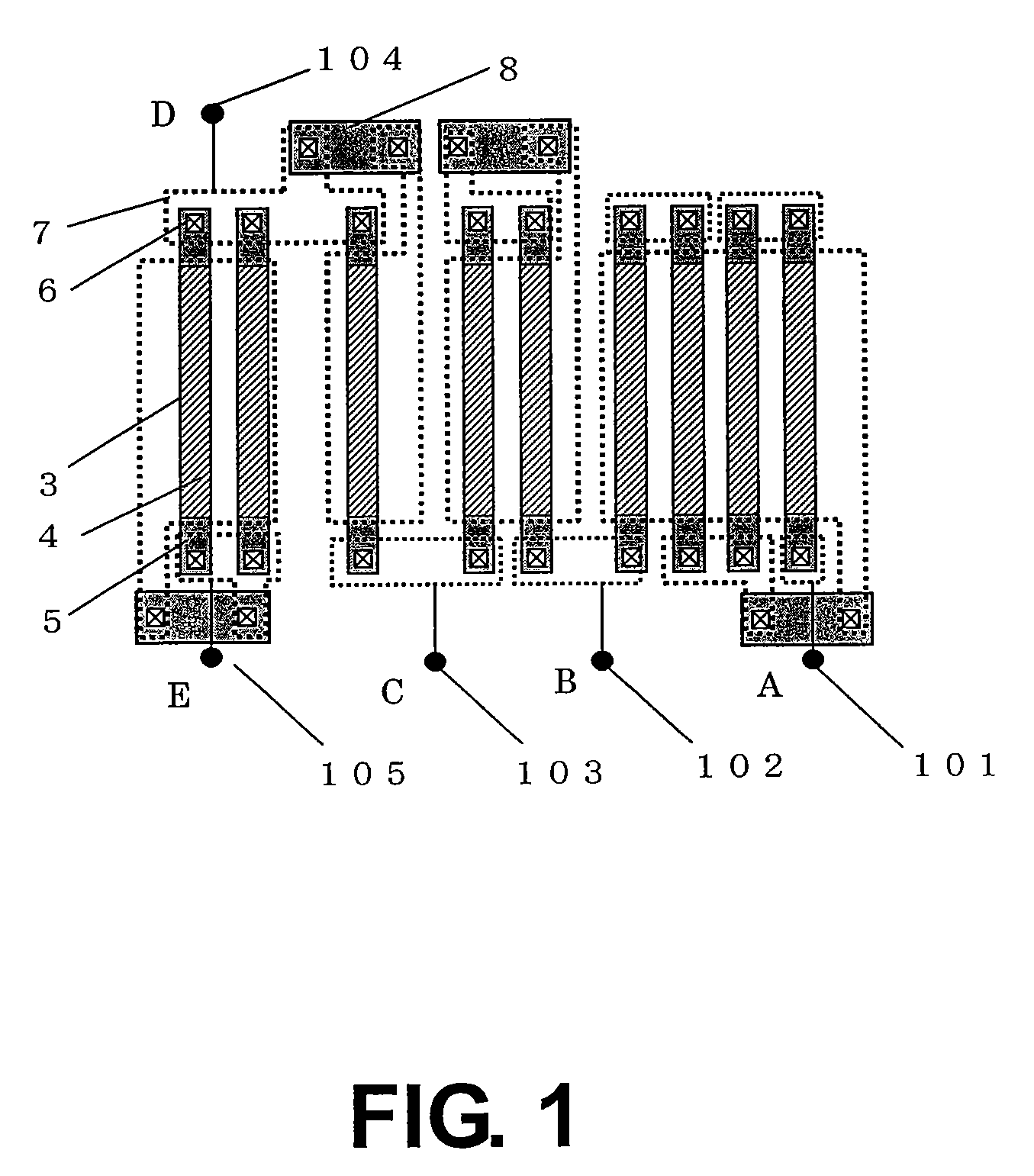
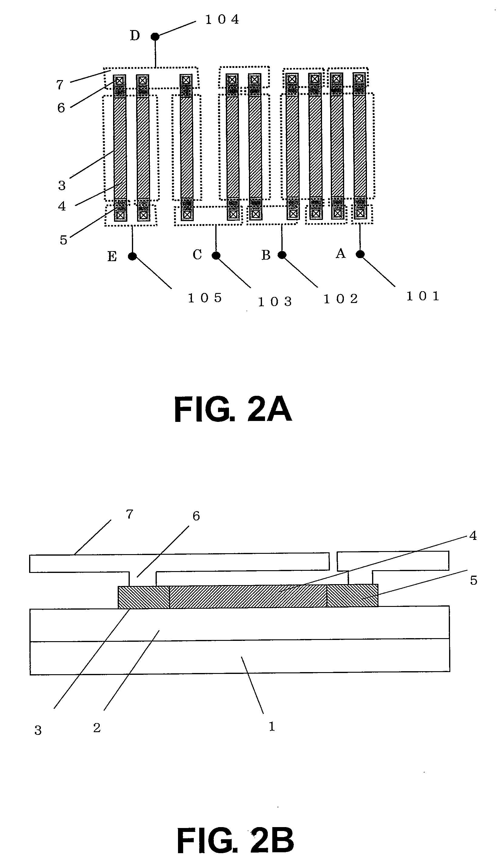
[0034]FIG. 5 is a cross-sectional view of a main portion illustrating the present invention for realizing the resistor circuit of FIG. 3. In this embodiment, an interconnecting layer for connecting a resistor and a metal line is made of polycrystalline silicon which is also used in the resistor. In this case, an additional step such as preparing an extra metal line layer is unnecessary, and providing a layout margin for alignment shift among different metal line layers is also unnecessary, resulting in requirement for a smaller area. In other words, the embodiment can cope with cost reduction, which is a great feature thereof. With regard to the disturbance noise, the resistance variation due to heat or charge is absorbed in the interconnecting layer made of polycrystalline silicon to thereby suppress its transmission to the resistor. Even the occurrence of the resistance variation in the interconnecting layer due to the influence of the disturbance noise does no harm to the circuit...

third embodiment

[0035]FIG. 6 is a cross-sectional view of a main portion according to the present invention for realizing the resistor circuit of FIG. 3. In this embodiment, it is assumed that a multi-layer metal line process is employed, in which an interconnecting layer for connecting a resistor and a metal line is formed of a second metal line provided on a third insulating film above the metal line which covers the resistor. As a result, just after formation of the metal line which covers the resistor, the metal line is not connected to anywhere and is in an electrically floating state, which has the advantage of causing no effect to the resistor immediately. Even when electric charges are accumulated in the metal line and are retained until the interconnecting layer formed of upper layer metal line is formed, the charges are dissipated from the semiconductor substrate or the stage electrically connected at a step of depositing metal for the upper layer metal line on the entire surface of a waf...


PUM


Abstract

A metal electrode is disposed on each of a plurality of resistor groups which are made of polycrystalline silicon resistors and constitute a resistor circuit. The metal electrode is connected to an end of the resistor via another interconnecting layer. Accordingly, the external influence which the metal electrode receives during a semiconductor manufacturing process is prevented from directly acting on the resistor, whereby resistance variation is suppressed.

Description

RELATED APPLICATIONS[0001]This application claims priority under 35 U.S.C. § 119 to Japanese Patent Application No. JP2007-326022 filed on Dec. 18, 2007, the entire content of which is hereby incorporated by reference.BACKGROUND OF THE INVENTION[0002]1. Field of the Invention[0003]The present invention relates to a semiconductor device including a resistor circuit made of polycrystalline silicon.[0004]2. Description of the Related Art[0005]In a semiconductor integrated circuit a diffusion layer resistor, which is made from a single crystalline silicon semiconductor substrate to which impurities of an opposite conductivity to the semiconductor substrate conductivity are introduced, and a polycrystalline silicon resistor, which is made of polycrystalline silicon to which impurities are introduced, are used. Of these, the polycrystalline silicon resistor is widely used in the semiconductor integrated circuit because of its advantages in, for example, a small leakage current due to an i...

Claims


Application Information

Patent Timeline
Patent Type & Authority Applications(United States)
IPC IPC(8): H01L29/8605
CPCH01L27/016H01L29/8605H01L27/1203H01L27/0802H01L27/04H01L21/822H01L21/28
Inventor HARADA, HIROFUMI
Owner ABLIC INC
Why Eureka
Try Eureka