Shock Wave and Power Generation Using on-Chip Nanoenergetic Material

Inactive Publication Date: 2009-06-18
UNIVERSITY OF MISSOURI
View PDF12 Cites 16 Cited by
  • Summary
  • Abstract
  • Description
  • Claims
  • Application Information

AI Technical Summary

Benefits of technology

[0008]Power is generated with this device is preferably used in pulsed power and continuous power application for portable device. The total power generation can be controlled by the device design and by the controlled ignition of the nano-engineered material. This allows for precise power control by the device.
[0009]The self-propagating reaction of the thermites allows power generation to proceed in a controlled manner. The combustion wave of the nanoenergetic material is realized in very small particles, but placement of the particles adjacent to one another allows the combustio

Problems solved by technology

One problem with this design is the eventual disposal of the device.
While the conversion itself does not produce any byproducts, the materials used for the device, such as HgCdTe and InSb, are toxic in nature.
Also, conventional microfabrication techniques cannot be applied to fabricate such a device.
Explosives are known to produce power

Method used


Image

  • Shock Wave and Power Generation Using on-Chip Nanoenergetic Material
  • Shock Wave and Power Generation Using on-Chip Nanoenergetic Material
  • Shock Wave and Power Generation Using on-Chip Nanoenergetic Material

Examples


example 1

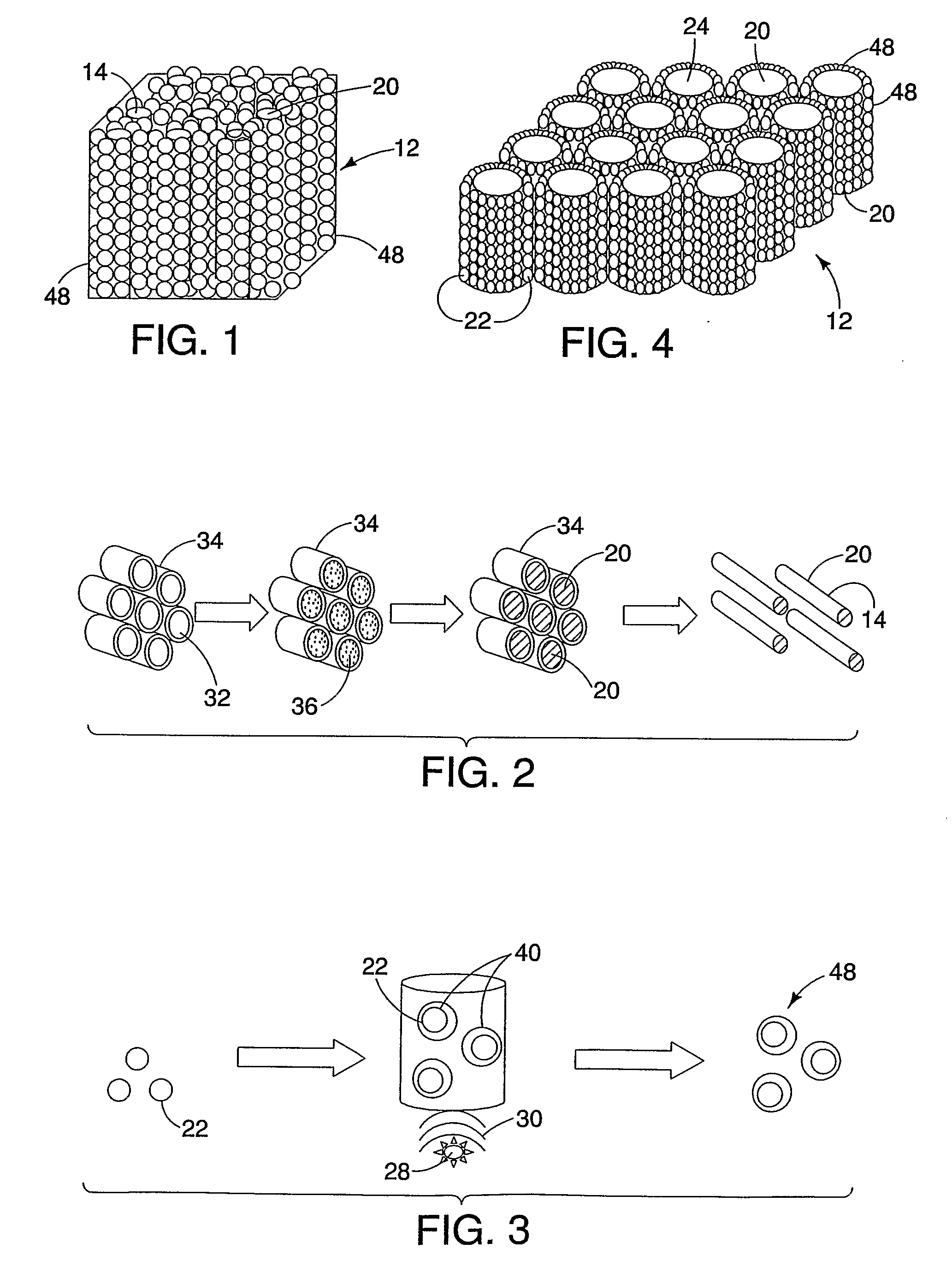
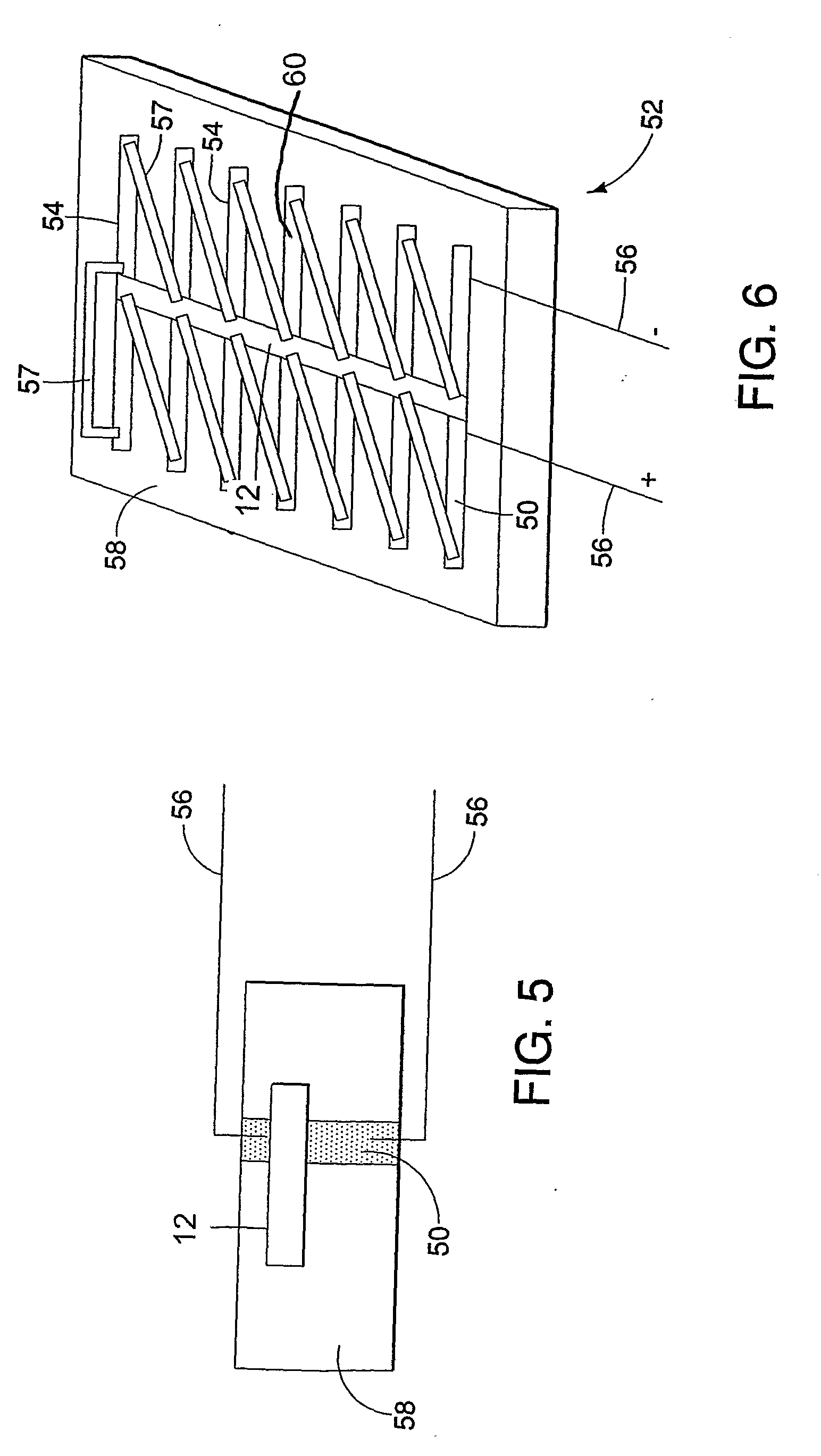
[0074]A device shown in FIG. 5 was fabricated where a clean glass substrate was coated with sputtered platinum film with Al wire connections on both sides for creating junctions and a dispersed thermite comprising nanorods of CuO and aluminum (wt.—10-20 mg) on one Pt / Al junction. An impact initiation was utilized to trigger a thermite reaction. A standard weight of 200 g was dropped from a height of 20 cm over the thermite. Due to a temperature differential between two Pt / Al junctions over the platinum film, voltage was generated, which was recorded using a data acquisition card (DAQ) and LabVIEW program. A voltage pulse of about 0.3 V peak voltage and 126 microsecond width at FWHM was generated using one Pt / Al (platinum film) transducer (FIG. 2). From the generated voltage value, the seebeck coefficient of platinum is calculated to be about 17 μV / ° C. This generated voltage of 0.3V is the open circuit voltage. To calculate the power and conversion efficiency, a load resistor is use...

example 2

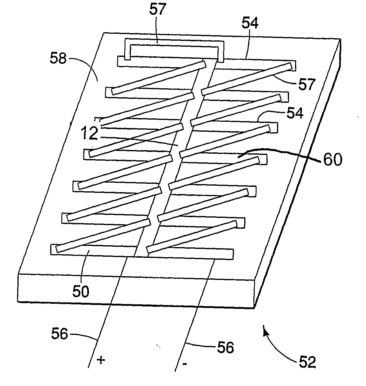
[0075]From our experiment of one platinum strip, the rise time of the open circuit output voltage is 100 μS and fall time is 360 μS. Total response time is 460 US. Taking the speed of the propagation of the energetic reaction of 2300 m / S, the reaction propagates 1380 mm in 460 μS. Taking the width of one platinum strip 3 mm and the gap between two strips 3 mm, the total number of platinum strips in 1380 mm is 230. In a device similar to the design of FIG. 6, 460 platinum strips are placed within that distance. By the time the generated voltage from first platinum strip goes zero the voltage of 460th platinum strip starts to rise. So 460 platinum strips work as a voltage generator connected in series at the same time. Because, all platinum strips do not generate equal voltage at the same time, the peak output voltage will be the sum of all 460 voltage generators and that is 0.3*460 / 2=69 V. More voltage is generated using thinner platinum strips which allow more strips within the dist...

example 3

[0077]A schematic of the millimeter scale device is shown in FIG. 8. Wells were made by gluing a thick LEXAN® brand polycarbonate substrate containing a pre-drilled through-hole to a glass substrate. The glass substrate had a sputtered thin-film heater composed of platinum on a titanium adhesion layer. The LEXAN® brand polycarbonate substrate is positioned such that the hole in it is aligned over the heating element of the Pt film. Leads are soldered to the metal film to allow connection to the heater. The hole was then packed with MIC powder using a Teflon spatula. The 5-15 mg of MIC material was a composite consisting of CuO nanorods with Al particles assembled on the surface of the nanorods. The diameter of the wells tested varied from 1.6 mm to 2.38 mm. A variation of this device can be made in which a thin elastic membrane can be placed over the opening of the well. In preliminary testing, a 1 mm thick polydimethylsiloxane (“PDMS”) membrane was glued on the top of the well afte...


PUM


Abstract

A method of generating power uses a nanoenergetic material. The nanoenergetic material comprising thermite is obtained and deposited on a substrate. An igniter is placed on the nanoenergetic material. When power is desired, the nanoenergetic material is ignited. A transducer receives thermal, sonic, magnetic, optic and/or mechanical energy from combustion of the nanoenergetic material and converts it into electrical energy. Preferably, the transducer is a thermoelectric, piezoelectric or magneto device. Preferably, multiple transducers are integrated in one power generators to maximize the power from nanoenergetic thermites.

Description

CROSS REFERENCE TO RELATED APPLICATION[0001]This application claims the benefit of U.S. Provisional Application 60 / 731,162, filed Oct. 28, 2005.TECHNICAL FIELD[0002]This invention deals with the power generation by the self-propagation of energetic materials. More specifically, it deals with the generation of power on a microchip that is converted to electrical energy.BACKGROUND ART[0003]Portable devices are very popular in our society. Common use of such devices demands the availability of portable source with which to power them. The variety of devices also demands that the power be accurately controlled. Even devices that are not portable benefit from the generation of power in a highly controlled manner. The power generators are operated while connected to an electrical storage unit such as a battery or a capacitor. Upon actuation, generated electrical pulses are delivered to a storage device. The storage device is then used as power source for another device.[0004]Research for ...

Claims


Application Information

Patent Timeline
IPC IPC(8): F03G7/00
CPCH01L35/30C06B45/14H10N10/13
Inventor GANGOPADHYAY, SHUBHRAAPPERSON, STEVENGANGOPADHYAY, KESHABBEZMELNITSYN, ANDREYTHIRUVENGADATHAN, RAJAGOPALANKRAUS, MICHAELSHENDE, RAJESHHOSSAIN, MARUFSUBRAMANIAN, SENTHILBHATTACHARYA, SHANTANUGAO, YUANGANG
Owner UNIVERSITY OF MISSOURI
Why Eureka
Try Eureka