Wiring substrate and display device including the same

Active Publication Date: 2009-06-18
SHARP KK
View PDF10 Cites 44 Cited by
  • Summary
  • Abstract
  • Description
  • Claims
  • Application Information

AI Technical Summary

Benefits of technology

[0009]In the wiring substrate according to a preferred embodiment of the present invention, a terminal portion and a wiring and a bump electrode that are adjacent to the terminal portion are effectively prevented from being short-circuited by the electrically conductive fine particles. Moreover, a bump electrode, and a bump electrode and a wiring that are adjacent to the bump electrode are effectively prevented from being short-circuited by the electrically conductive fine particles. Accordingly, generation of leakage current can be effectively suppressed by the present preferred embodiment of the present invention.
[0037]In the second display device according to a preferred embodiment of the present invention, a terminal portion and a wiring and a bump electrode that are adjacent to the terminal portion can be effectively prevented from being short-circuited by the electrically conductive fine particles. Moreover, a bump electrode and a bump electrode and a wiring that are adjacent to the bump electrode can be effectively prevented from being short-circuited by the electrically conductive fine particles. Accordingly, generation of leakage current can be effectively prevented by preferred embodiments of the present invention. As a result, a display device having high electrical reliability can be provided.

Problems solved by technology

However, in the case where an IC chip is flip chip mounted with an ACF or ACP, adjacent terminals and bump electrodes are short-circuited by electrically conductive fine particles included in the ACF and the like, causing a leakage current.
Adjacent terminals and bump electrodes are likely to be short-circuited especially in the case where a fine-pitch IC chip having closely spaced bump electrodes is mounted.
Therefore, in the liquid crystal display device of Japanese Laid-Open Patent Publication No. 9-244047, adjacent bump electrodes may be short-circuited by electrically conductive fine particles and generation of leakage current is not sufficiently suppressed.

Method used


Image

  • Wiring substrate and display device including the same
  • Wiring substrate and display device including the same
  • Wiring substrate and display device including the same

Examples


first preferred embodiment

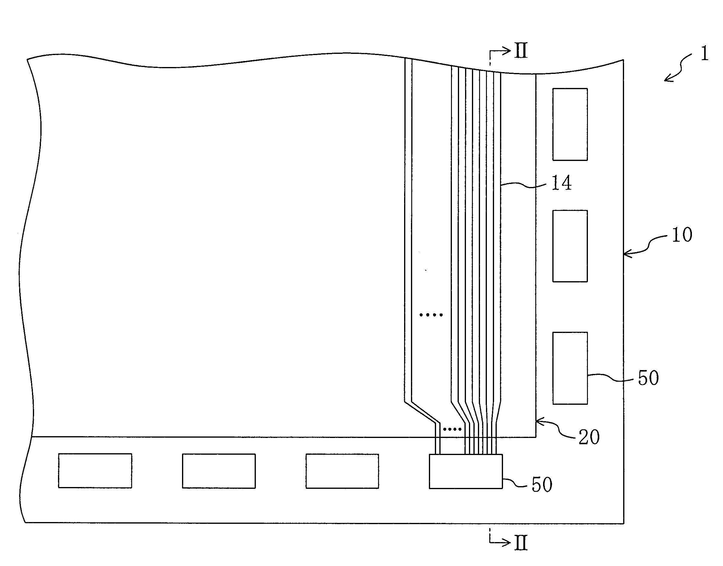
[0062]FIG. 1 is a plan view of a liquid crystal display device 1 according to a first preferred embodiment of the present invention.

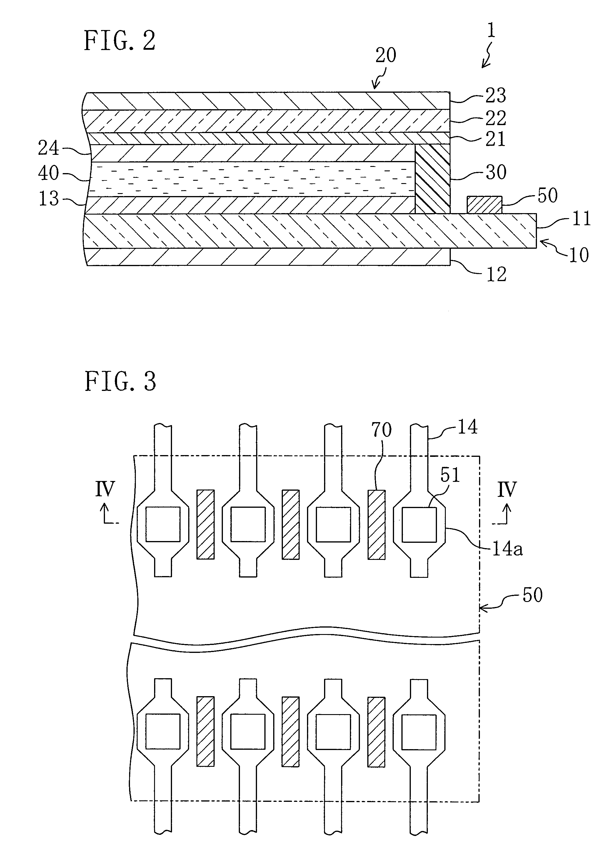
[0063]FIG. 2 is a cross-sectional view taken along line II-II in FIG. 1.

[0064]The liquid crystal display device 1 of the first preferred embodiment preferably includes an active matrix substrate 10, a counter substrate 20 facing the active matrix substrate 10, a liquid crystal layer 40 interposed between the active matrix substrate 10 and the counter substrate 20 as a display medium layer, and a seal member 30 bonding the active matrix substrate 10 and the counter substrate 20 to each other and sealing the liquid crystal layer 40.

[0065]The active matrix substrate 10 has a first substrate 11 made of plastic or glass and a first polarizing plate 12 provided on the opposite side to the liquid crystal layer 40 on the first substrate 11. A plurality of gate lines and a plurality of source lines are provided on the active matrix substrate 10. The plurality of...

second preferred embodiment

[0086]FIG. 5 is an enlarged plan view of a region around a driving IC chip 50 of a liquid crystal display device according to a second preferred embodiment.

[0087]FIG. 6 is a cross-sectional view taken along line XI-XI in FIG. 5.

[0088]The liquid crystal display device of the second preferred embodiment preferably has the same structure as that of the liquid crystal display device 1 of the first preferred embodiment except for the arrangement of the insulating members 70, the terminal portions 14a, and the bump electrodes 51. The arrangement of the insulating members 70, the terminal portions 14a, and the bump electrodes 51 of the second preferred embodiment will now be described in detail with reference to FIGS. 5 and 6. Note that FIGS. 1 and 2 referred to in the first preferred embodiment are also referred to in the second preferred embodiment. Elements having substantially the same function as in the first preferred embodiment will be denoted by the same reference numerals and char...

third preferred embodiment

[0094]FIG. 9 is an enlarged cross-sectional view of a region around a driving IC chip 50 of a liquid crystal display device according to a third preferred embodiment.

[0095]The liquid crystal display device of the third preferred embodiment preferably has the same structure as that of the liquid crystal display device of the second preferred embodiment except for the arrangement of the insulating members 70. The arrangement of the insulating members 70 of the third preferred embodiment will be described in detail with reference to FIG. 9. Note that FIGS. 1, 2, and 5 referred to in the second preferred embodiment are also referred to in the third preferred embodiment. Elements having substantially the same function as in the second preferred embodiment will be denoted by the same reference numerals and characters and description thereof will be omitted.

[0096]In the third preferred embodiment, the insulating members 70 are arranged in contact with both the active matrix substrate 10 an...


PUM


Abstract

An active matrix substrate includes a first substrate, a driving integrated circuit chip mounted on the first substrate with an anisotropic electrically conductive layer, and an insulating member. The insulating member isolates a terminal from a wiring and a bump electrode that are adjacent to the terminal portion and isolates a bump electrode facing the terminal portion from a bump electrode and a wiring that are adjacent to the bump electrode.

Description

BACKGROUND OF THE INVENTION[0001]1. Field of the Invention[0002]The present invention relates to a wiring substrate and a display device including the same.[0003]2. Description of the Related Art[0004]In recent years, a flip chip mounting method using an anisotropic electrically conductive film (hereinafter, sometimes referred to as “ACF”) or an anisotropic electrically conductive paste (hereinafter, sometimes referred to as “ACP”) or the like has been widely used as a method for mounting an integrated circuit chip (hereinafter, sometimes referred to as an “IC chip”) to a wiring substrate. See, for example, Japanese Laid-Open Patent Publication No. 9-244047.[0005]However, in the case where an IC chip is flip chip mounted with an ACF or ACP, adjacent terminals and bump electrodes are short-circuited by electrically conductive fine particles included in the ACF and the like, causing a leakage current. Adjacent terminals and bump electrodes are likely to be short-circuited especially i...

Claims


Application Information

Patent Timeline
IPC IPC(8): H05K7/00H05K1/16G02F1/1333
CPCG02F1/13452H01L2224/83851H01L24/17H01L24/28H01L24/31H01L24/83H01L2224/13099H01L2224/16225H01L2224/73204H01L2224/838H01L2924/01005H01L2924/01057H01L2924/01058H01L2924/0781H01L2924/14H05K3/323H05K3/3452H05K2201/09709H05K2201/09909H05K2201/10674H05K2203/167H01L2924/01006H01L2924/01033H01L2924/0665H01L24/12H01L2224/8114H01L2224/29499H01L2224/26152H01L2224/83136H01L2224/83139H01L2224/8314H01L2224/2919H01L2924/00H01L2924/15788
Inventor YAMASHITA, KENICHIAITA, TETSUYA
Owner SHARP KK
Why Eureka
Try Eureka