Supercharge Your Innovation With Domain-Expert AI Agents!

Methods for manufacturing CMOS compatible bio-sensors

a bio-sensor and manufacturing method technology, applied in the field of manufacturing methods for cmos compatible bio-sensors, can solve the problems of long etching time for lateral etching metal, low process yield and process cost, and fixed suspension height, and achieve the effect of facilitating electronic circuit integration

Inactive Publication Date: 2009-06-18
NAT APPLIED RES LAB
View PDF9 Cites 0 Cited by
  • Summary
  • Abstract
  • Description
  • Claims
  • Application Information

AI Technical Summary

Benefits of technology

[0003]One of the objectives of the present invention is to provide a manufacture method for CMOS biosensor, more specifically, a manufacture method for CMOS sensor having suspension arm structure which allows the formation of biosensor layer needed by the biosensor on silicon dioxide or conductive metal according to the need; in the same process, suspension arm structures of different thicknesses are made according to different design; moreover, process compatible with CMOS device is used to facilitate the electronic circuit integration.

Problems solved by technology

However, the metal and other sensing film commonly used in the biosensor is not frequently used in general CMOS electronic device; therefore, some drawbacks are caused, for example, process design difficulty, process yield drop and process cost increase.
However, some drawbacks can be seen, for example, long etching time for lateral etching metal and the suspension height is fixed since the conductive metal is of fixed thickness.
Therefore the movement stroke of suspension arm structure is then fixed and can not be utilized in several ways.

Method used


Image

  • Methods for manufacturing CMOS compatible bio-sensors
  • Methods for manufacturing CMOS compatible bio-sensors
  • Methods for manufacturing CMOS compatible bio-sensors

Examples


Embodiment Construction

[0010]The present invention will be described in the followings by different embodiments, and the components, arrangements and steps used to describe the content of this embodiment are only examples and are not used to limit this invention. In addition, “and / or” used in the disclosed content is for briefing purpose; the descriptions of “covering” or “above” can include the direct contact and no direct contact.

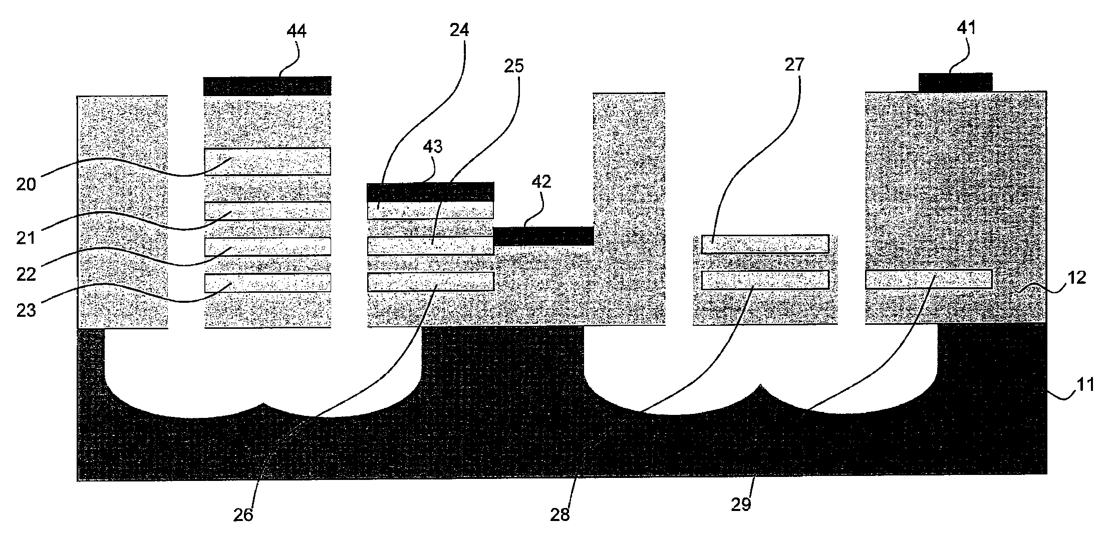
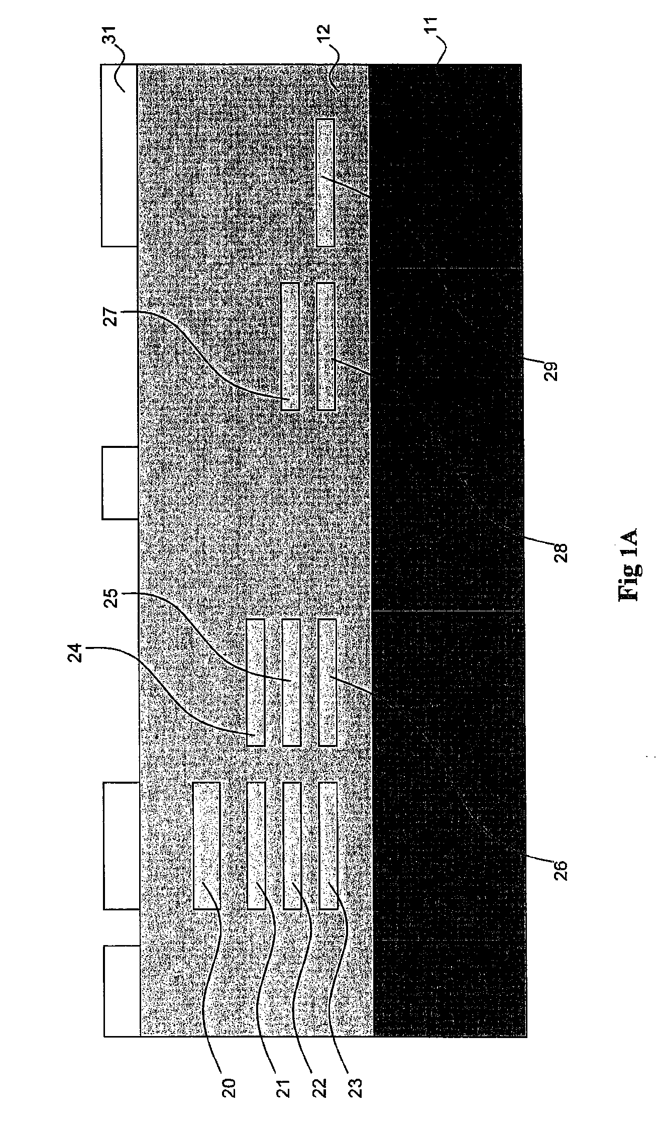
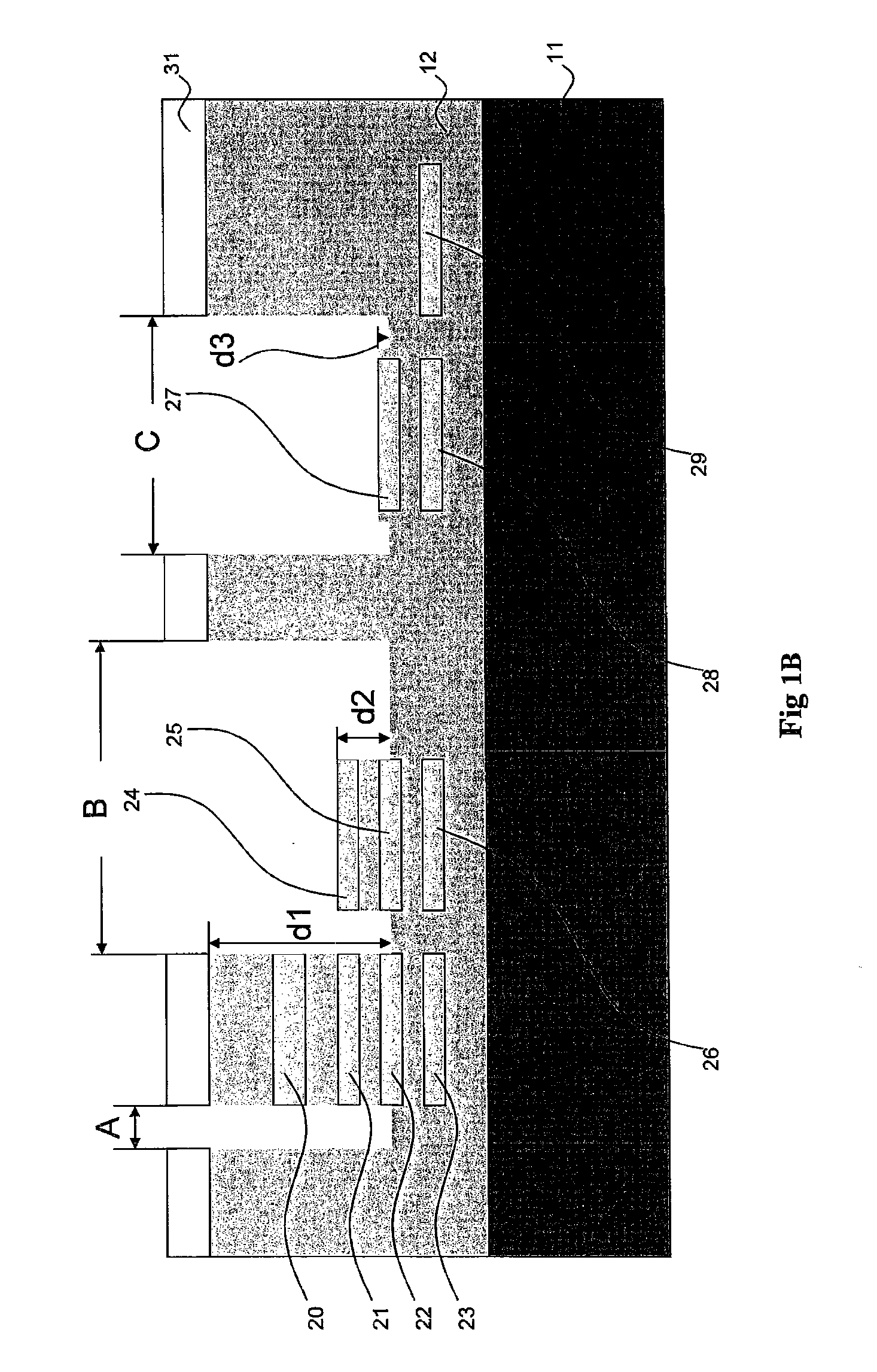
[0011]FIG. 1A˜1I shows a flow chart of the manufacture method of CMOS biosensor of the first embodiment of the present invention. FIG. 1A shows, through the use of semiconductor processes such as: Chemical Vapor Deposition (CVD), Physical Vapor Deposition (PVD), Photo Resist Coating, Photolithography, Dry Etching and Wet Etching, the formation of multiple device structural layers such as 20, 21, 22, 23, 24, 25, 26, 27, 28, 29 so as to form CMOS structure and Biosensor structure (not shown in the figure). On the substrate, protection layer 12 and first patterned photo resist lay...


PUM


Abstract

A manufacture method for CMOS sensor, which comprise of steps such as: forming protection layer on a substrate having multiple device structural layers, then using first photo-resist layer as mask for etching to form patterned molecular sensing layer, then forming third photo resist layer and etching protection layer and substrate so as to remove partial substrate underneath the sensor structure.

Description

FIELD OF THE INVENTION[0001]The present invention is related to a manufacture method for CMOS (Complementary Metal Oxide Semiconductor, CMOS) compatible sensor, it specifically relates to a manufacture method for CMOS compatible sensors for sensing Biological or ions concentration.BACKGROUND OF THE INVENTION[0002]CMOS biosensor is to design biosensor with CMOS electronic device on the same chip, which is thus a process that can integrate biosensor and CMOS electronic device. However, the metal and other sensing film commonly used in the biosensor is not frequently used in general CMOS electronic device; therefore, some drawbacks are caused, for example, process design difficulty, process yield drop and process cost increase. For the prior art process of using CMOS device to prepare suspension structure, please refer to U.S. Pat. No. 6,396,368, which uses conductive metal, for example, aluminum copper, as a sacrificial layer. However, some drawbacks can be seen, for example, long etc...

Claims


Application Information

Patent Timeline
IPC IPC(8): H01L21/8238
CPCB81B2201/0214B81C1/00246B81C2203/0714G01N27/128B81C2203/0735
Inventor LIN, CHEN-FUTSAI, HANN-HUEIJUANG, YING-ZONGCHIU, CHIN-FONG
Owner NAT APPLIED RES LAB
Features
  • R&D
  • Intellectual Property
  • Life Sciences
  • Materials
  • Tech Scout
  • Unparalleled Data Quality
  • Higher Quality Content
  • 60% Fewer Hallucinations
Learn More