Through hole capacitor and method of manufacturing the same

a technology of capacitors and through holes, which is applied in the direction of variable capacitors, feed-through capacitors, printed circuit non-printed electric components association, etc., can solve the problems of increasing the manufacturing cost, and increasing the number of pins for connecting other elements on the outside. , to achieve the effect of improving the voltage stabilizing effect and significantly increasing the capacitor through hol

Active Publication Date: 2009-06-25
IND TECH RES INST
View PDF14 Cites 18 Cited by
  • Summary
  • Abstract
  • Description
  • Claims
  • Application Information

AI Technical Summary

Benefits of technology

[0014]As the present invention increases the surface area of the dielectric layer in the through hole capacitor, the capacitance of the through hole capacitor is significantly increased. Furthermore, the embedded through hole capacitor of the present invention is closer to IC requiring a stable voltage than the conventional SMD capacitor, thus achieving better voltage stabilizing effect.

Problems solved by technology

With the increasingly complicated functions of IC, the number of pins for connecting other elements on the outside is increased, such that the wiring of the circuit board gets more and more complex, and the installation of the SMD capacitor also occupies the surface area of the IC substrate.
Therefore, a circuit board with more layers is required or the area of the circuit board is required to be increased, thus increasing the manufacturing cost.
With the increasing layers of the stack, the conventional arrangement of SMD capacitors on the circuit board is no longer able to stabilize the voltage in multiple chip stacking.

Method used


Image

  • Through hole capacitor and method of manufacturing the same
  • Through hole capacitor and method of manufacturing the same
  • Through hole capacitor and method of manufacturing the same

Examples


first embodiment

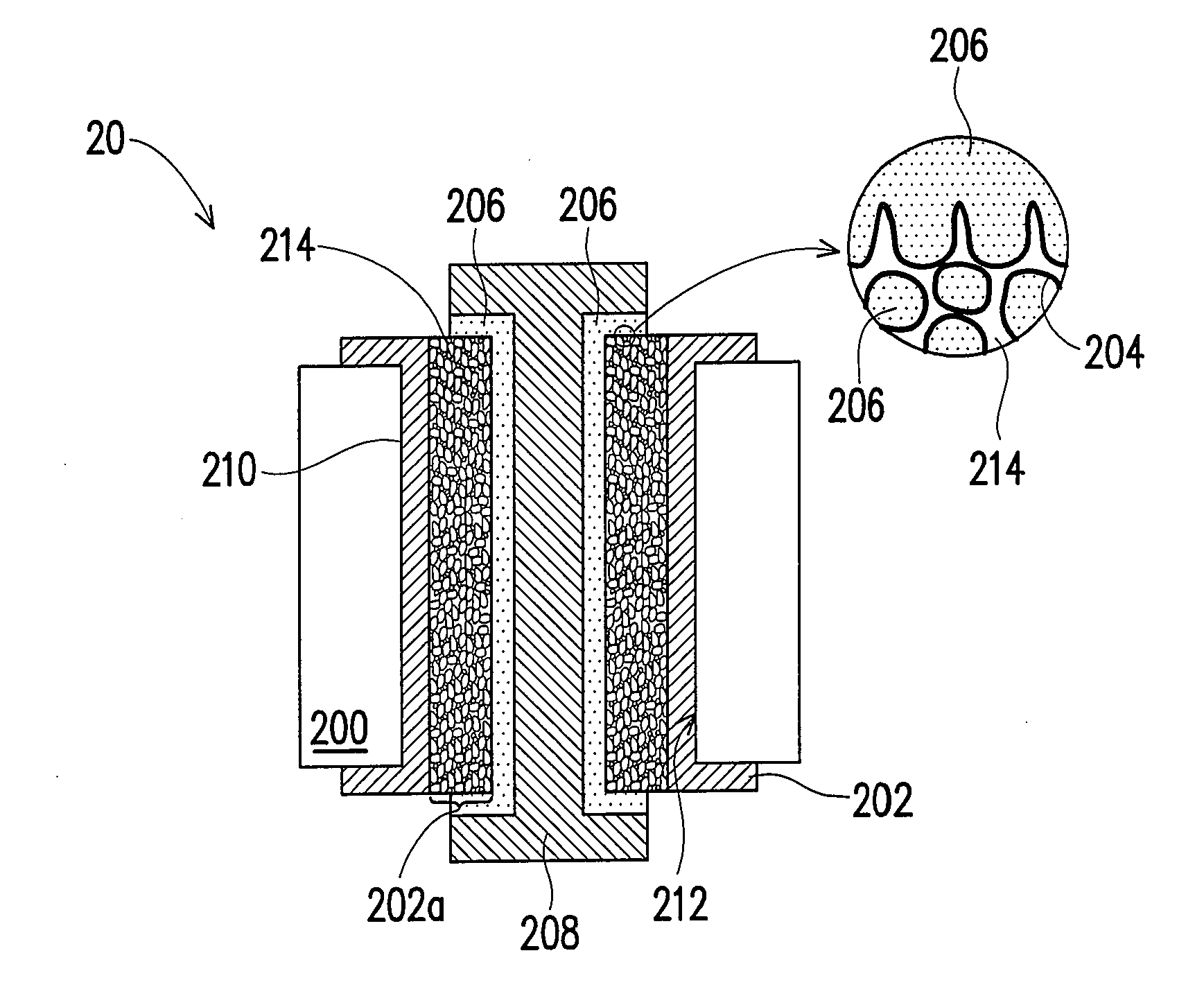
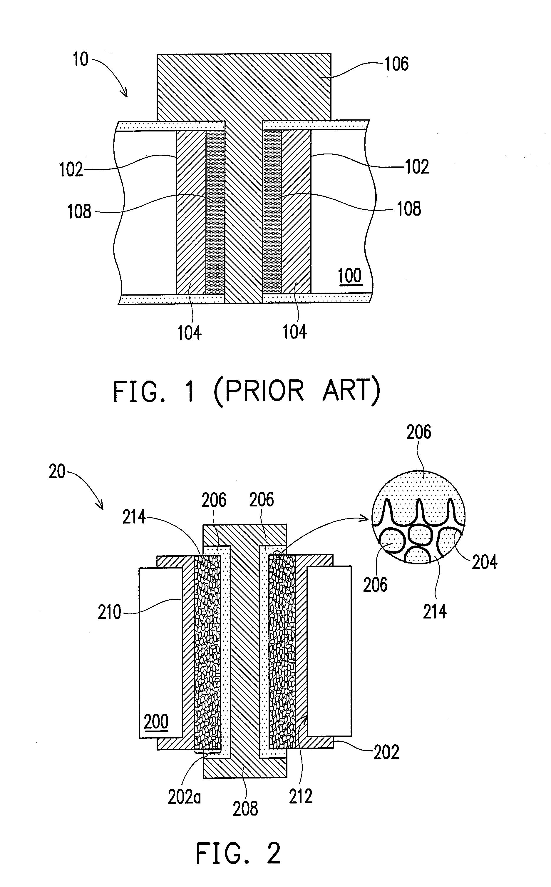
[0023]FIG. 2 is a schematic cross-sectional view of a through hole capacitor according to the present invention.

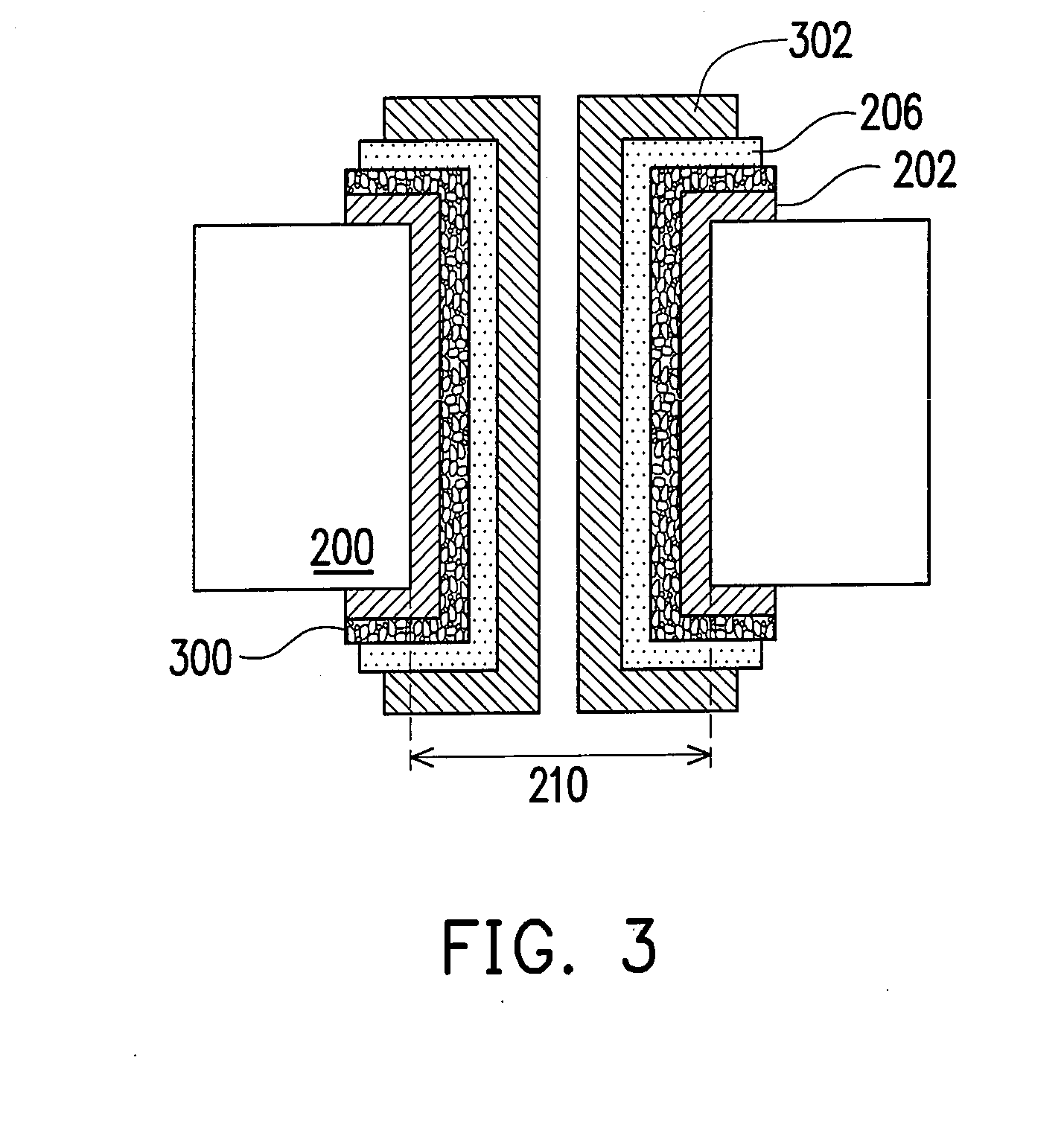
[0024]Referring to FIG. 2, a through hole capacitor 20 of the first embodiment includes a substrate 200, an anode layer 202, a dielectric layer 204, a first cathode layer 206, and a second cathode layer 208. The substrate 200 has a through hole 210. In the first embodiment, the substrate 200 is a silicon substrate and can further be an insulating substrate or a metal substrate. Although merely one through hole 210 and one through hole capacitor 20 are shown in FIG. 2, the substrate 200 can further has other through holes, which can be disposed with the through hole capacitors and can further serve as a portion of the circuit wiring. Further, a plurality of through hole capacitors can be connected in parallel to one another completely or partially. The through holes in the substrate can be arranged in an array. Furthermore, the first embodiment is described with a cross sec...

second embodiment

[0029]FIG. 4 is a flow chart of manufacturing processes of a through hole capacitor according to the present invention.

[0030]Referring to FIG. 4, in Step 400, a plurality of through holes is formed in a substrate. The substrate is, for example, a silicon substrate, an insulating substrate, or a metal substrate.

[0031]In Step 402, an anode layer is formed on an inner surface of at least one through hole. A material of the anode layer is, for example, aluminum, tantalum, niobium, or niobium monoxide.

[0032]Next, in Step 404, a surface treatment is performed on the anode layer to make a surface of the anode layer be a porous structure. The surface treatment is, for example, an etching process or another process capable of roughening the surface of the anode layer. For example, when the material of the anode layer is aluminum, etching can be performed by using hydrochloric acid, sulfuric acid, phosphoric acid, or a mixture thereof.

[0033]In Step 406, a dielectric layer is formed on the por...


PUM

PropertyMeasurementUnit
structureaaaaaaaaaa
conductivityaaaaaaaaaa
conductiveaaaaaaaaaa

Abstract

A through hole capacitor at least including a substrate, an anode layer, a dielectric layer, a first cathode layer, and a second cathode layer is provided. The substrate has a plurality of through holes. The anode layer is disposed on the inner surface of at least one through hole, and the surface of the anode layer is a porous structure. The dielectric layer is disposed on the porous structure of the anode layer. The first cathode layer covers a surface of the dielectric layer. The second cathode layer covers a surface of the first cathode layer, and the conductivity of the second cathode layer is greater than that of the first cathode layer. The through hole capacitor can be used for impedance control, as the cathode layers of the through hole are used for signal transmission.

Description

CROSS-REFERENCE TO RELATED APPLICATION[0001]This application claims the priority benefit of Taiwan application serial no. 96149239 on Dec. 21, 2007. The entirety the above-mentioned patent application is hereby incorporated by reference herein and made a part of specification.BACKGROUND OF THE INVENTION[0002]1. Field of the Invention[0003]The present invention generally relates to a through hole capacitor capable of improving capacitance and a method of manufacturing the same.[0004]2. Description of Related Art[0005]Capacitors on a circuit board are mostly surface mounted device (SMD) elements in conventional art, which are fixed on pads fixed on the circuit board.[0006]With the increasingly complicated functions of IC, the number of pins for connecting other elements on the outside is increased, such that the wiring of the circuit board gets more and more complex, and the installation of the SMD capacitor also occupies the surface area of the IC substrate. Therefore, a circuit boar...

Claims


Application Information

Patent Timeline
Patent Type & Authority Applications(United States)
IPC IPC(8): H05K1/18H01G4/35
CPCH01G9/012H05K1/162H05K2201/09809Y10T29/417Y02E60/13H01G11/48Y10T29/435H05K2203/0315
Inventor WU, BANG-HAOTSAI, LI-DUANLEE, MIN-LINCHENG, CHENG-LIANG
Owner IND TECH RES INST
Why Eureka
Try Eureka