Nanotubes and nanowires based electronic devices and method of fabrication thereof

a technology of nanowires and electronic devices, applied in the field of biomolecular electronics, can solve the problems of low yield, achieve the effect of facilitating mass production of such devices, high efficiency, and facilitating the production of self-assembled nanostructures

Inactive Publication Date: 2009-06-25
YEDA RES & DEV CO LTD
View PDF8 Cites 24 Cited by
  • Summary
  • Abstract
  • Description
  • Claims
  • Application Information

AI Technical Summary

Benefits of technology

[0058]There is a need in the art to facilitate production of self-assembled nanostructures based devices with high efficiency, especially in a manner facilitating mass production of such devices. This is associated with the fact that the known techniques of the kind specified, despite their ability to fabricate single-walls carbon nanotube based devices, involve multiple production steps resulting in low yield.

Problems solved by technology

This is associated with the fact that the known techniques of the kind specified, despite their ability to fabricate single-walls carbon nanotube based devices, involve multiple production steps resulting in low yield.

Method used


Image

  • Nanotubes and nanowires based electronic devices and method of fabrication thereof
  • Nanotubes and nanowires based electronic devices and method of fabrication thereof
  • Nanotubes and nanowires based electronic devices and method of fabrication thereof

Examples


Embodiment Construction

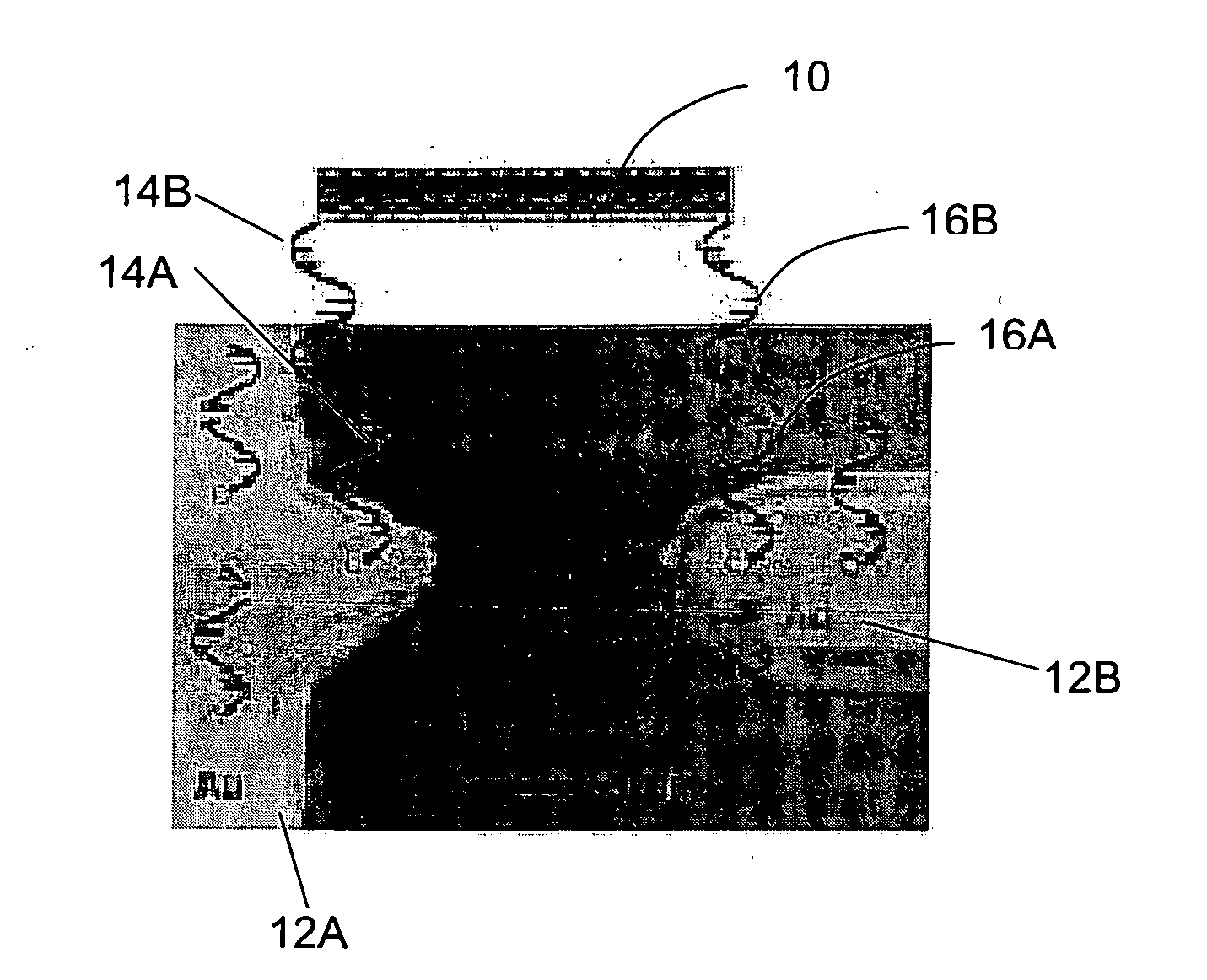
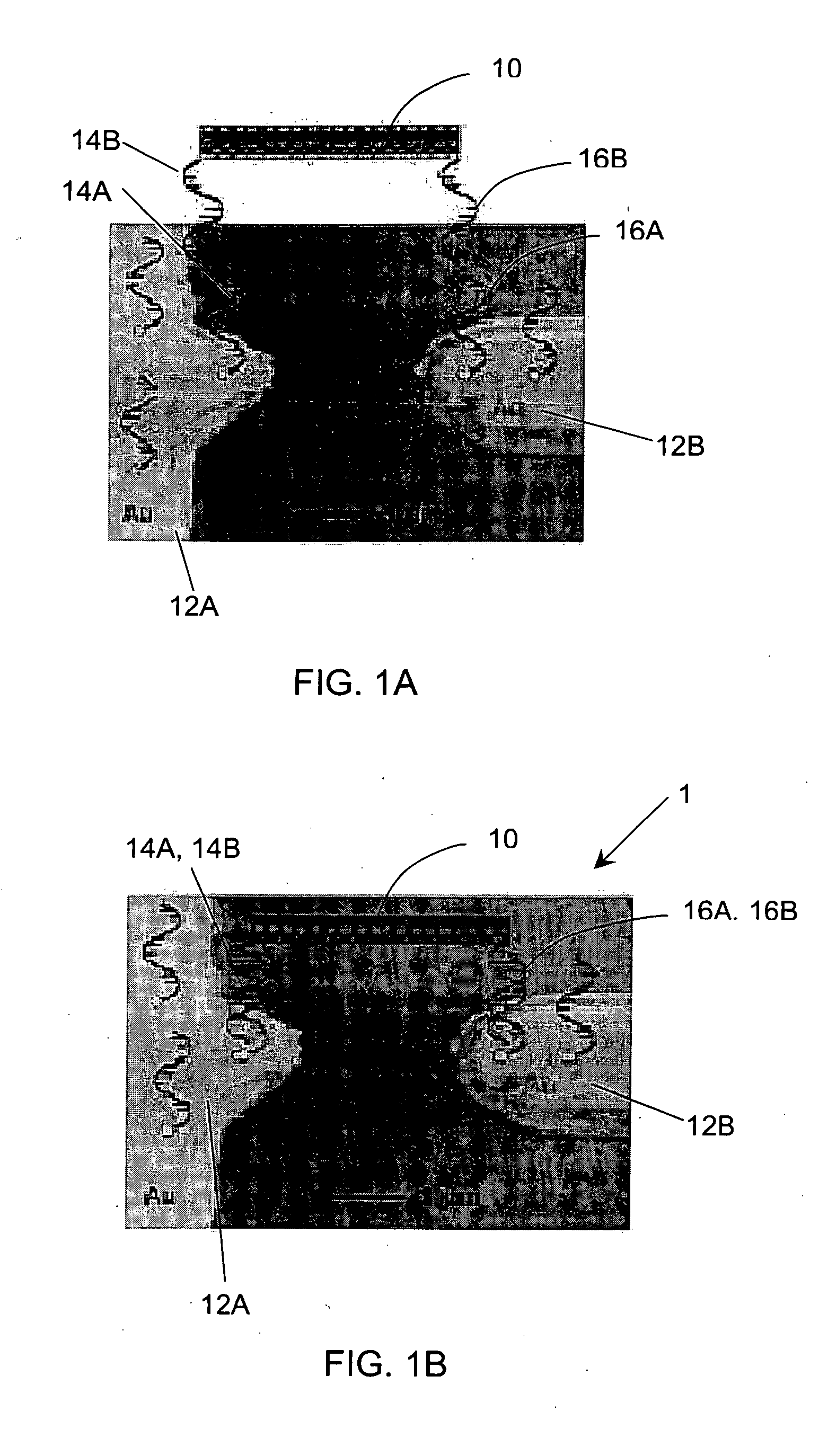
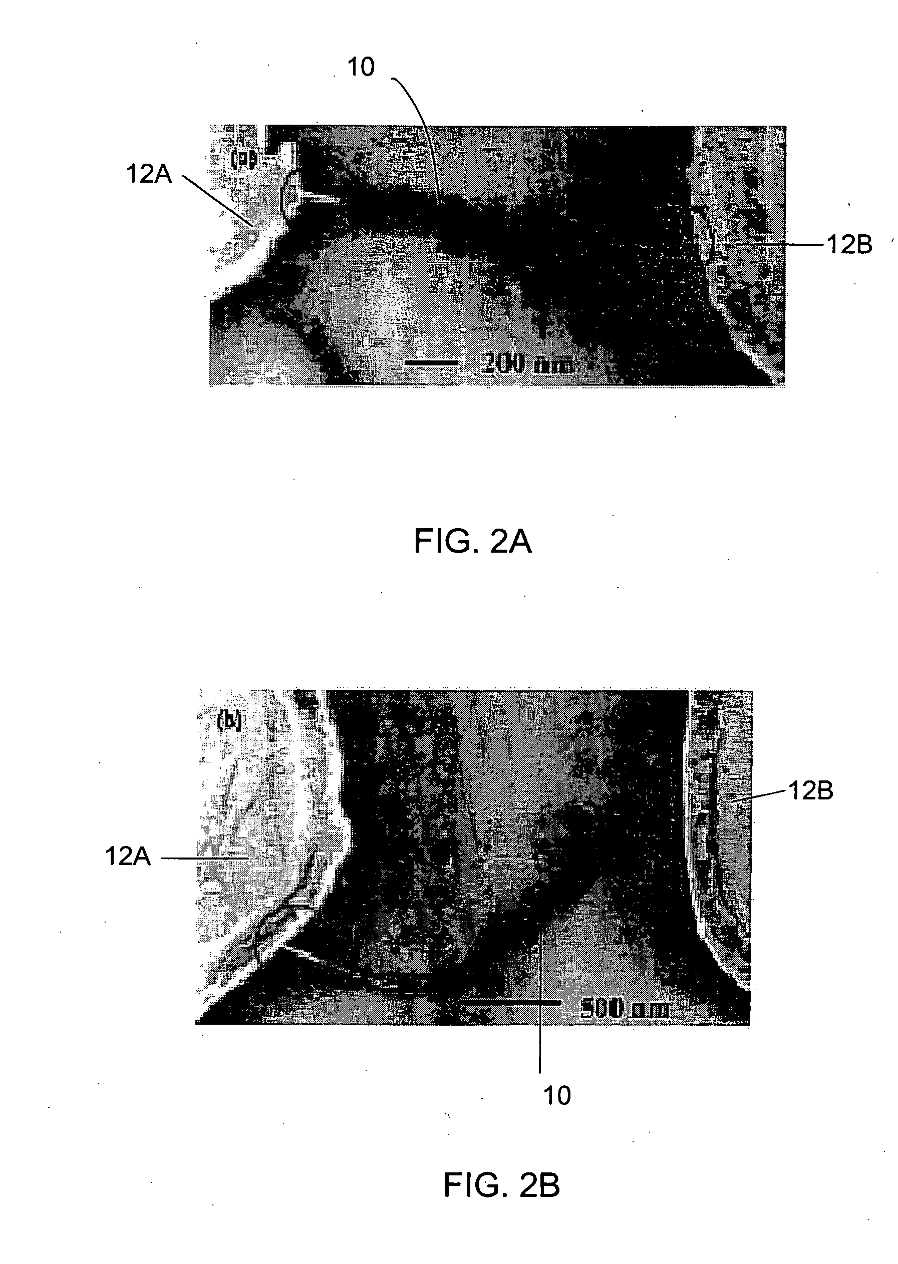
[0102]Referring to FIGS. 1A and 1B, there is exemplified a nanotube based (carbon and / or inorganic semiconductor nanotube) electronic device of the present invention and a method of its fabrication. In the present example, a carbon nanotube based device is considered. It should be noted that the term “nanotube” used in the description below refers also to a nanowire and nanotubes' and / or nanowires' bundle.

[0103]As shown in FIG. 1B, an electronic device 1 is formed by a carbon nanotube 10 interconnected between two electrodes 12A and 12B (gold electrodes in the present example) via a biological binder formed by nucleic acid bindings 14A-14B and 16A-16B, being binding biological moieties that serve as chemical linkers.

[0104]As indicated above, the biological moiety according to the present invention may be any biological moiety of the kind that is known to specifically interact with another recognizable moiety, which may or may not be a biological moiety. In the context of this invent...


PUM

PropertyMeasurementUnit
currentsaaaaaaaaaa
gate voltageaaaaaaaaaa

Abstract

An electronic device is presented comprising at least one electrically conductive element coupled to an elongated carbon or inorganic semiconductor based nanostructure, by a biological binder.

Description

FIELD OF THE INVENTION[0001]This invention is generally in the field of biomolecular electronics, and relates to a nanotubes or nanowires based electronic device and method of its fabrication.LIST OF REFERENCES[0002]The following references are considered to be pertinent for the purpose of understanding the background of the present invention:[0003][1] S. G. Rao, L. Huang, W. Setyawan, S. Hong, Nature 425 (2003) 36;[0004][2] B. Kim, W. M. Sigmund, Langmuir 19 (2003) 4848;[0005][3] G. Xia, H. Tengjiao, L. Luqi, G. Zhixin, Chem. Phys. Lett. 370 (2003) 661;[0006][4] Z. Liu, Z. Shen, J. Zhu, S. Hou, L. Ying, Z. Shi, Z. Gu, Langmuir 16 (2000) 3569;[0007][5] H. Xin, A. T. Wooley, J. Am. Chem. Soc. 125 (2003) 8710;[0008][6] K. Keren, R. S. Berman, E. Buchstab, U. Sivan, E. Braun, Science 302 (2003) 1380;[0009][7] M. Hazani, R. Naaman, F. Hennrich, M. M. Kappes, Nano Lett. 3 (2003) 153;[0010][8] M. S. Strano, C. A. Dyke, M. L. Usrey, P. W. Barone, M. J. Allen, H. Shan, C. Kittrell, R. H. Ha...

Claims


Application Information

Patent Timeline
Patent Type & Authority Applications(United States)
IPC IPC(8): C12M1/00G01N27/00
CPCB82Y10/00B82Y30/00G11C13/0014G11C13/0019G01N27/4146G11C2213/16G11C2213/17G01N27/4145G11C13/025
Inventor NAAMAN, RONHAZANI, MIRONSHVARTS, DMITRYPELED, DANASIDORIV, VICTOR
Owner YEDA RES & DEV CO LTD
Why Eureka
Try Eureka