Supercharge Your Innovation With Domain-Expert AI Agents!

Semiconductor device and photomask

a technology applied in the field of semiconductor devices and photomasks, to achieve the effect of suppressing the generation of opening defects

Active Publication Date: 2009-07-02
RENESAS ELECTRONICS CORP
View PDF7 Cites 6 Cited by
  • Summary
  • Abstract
  • Description
  • Claims
  • Application Information

AI Technical Summary

Benefits of technology

[0007]In view of the foregoing, an object of the invention is to provide a semiconductor device and a photomask that can suppress the opening defect of the shared contact hole.
[0010]In the semiconductor device of the aspect of the invention, in the planar view, the second sidewall in the portion that the shared contact hole of the gate electrode layer reaches is shifted toward sides of the third and fourth sidewalls from the virtual extended line of the first sidewall in the portion located on the channel formation region of the gate electrode layer. Therefore, a distance between the second sidewall in the portion that the shared contact hole of the gate electrode layer reaches and the edge of the shared contact hole can be increased to suppress the generation of the opening defect during the etching in making the shared contact hole.

Problems solved by technology

The reduction of the etching area obstructs the progress of the etching, resulting in a conductive problem such as an opening defect in which the shared contact hole does not reach an active layer (impurity region).

Method used


Image

  • Semiconductor device and photomask
  • Semiconductor device and photomask
  • Semiconductor device and photomask

Examples


first embodiment

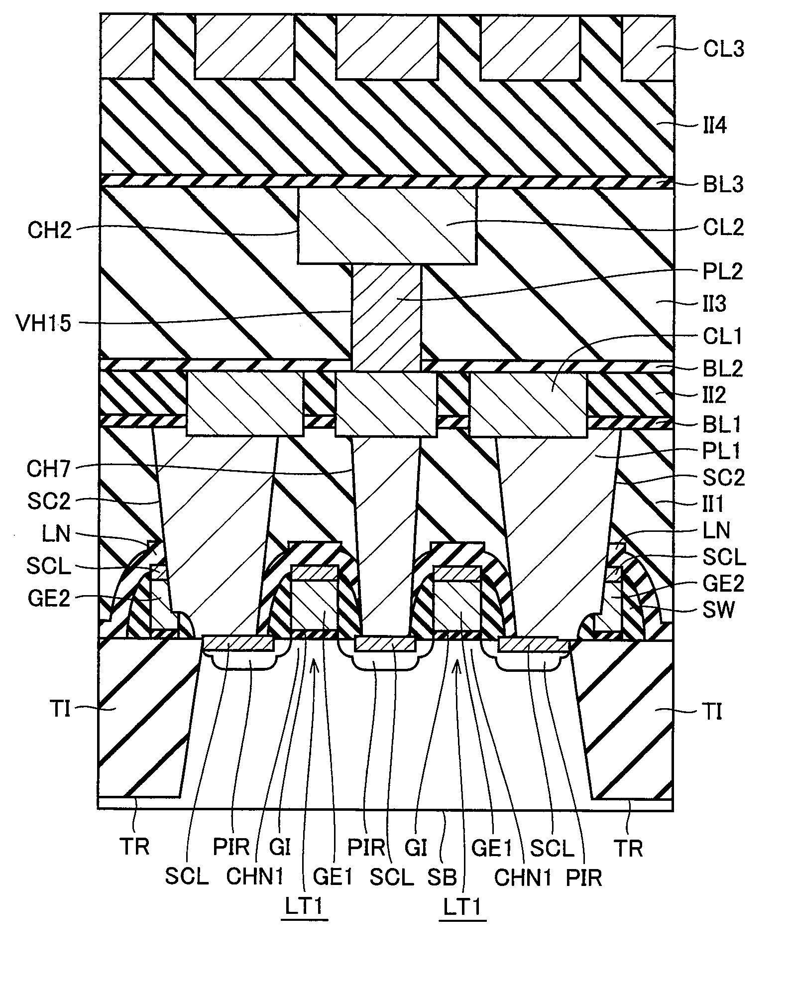
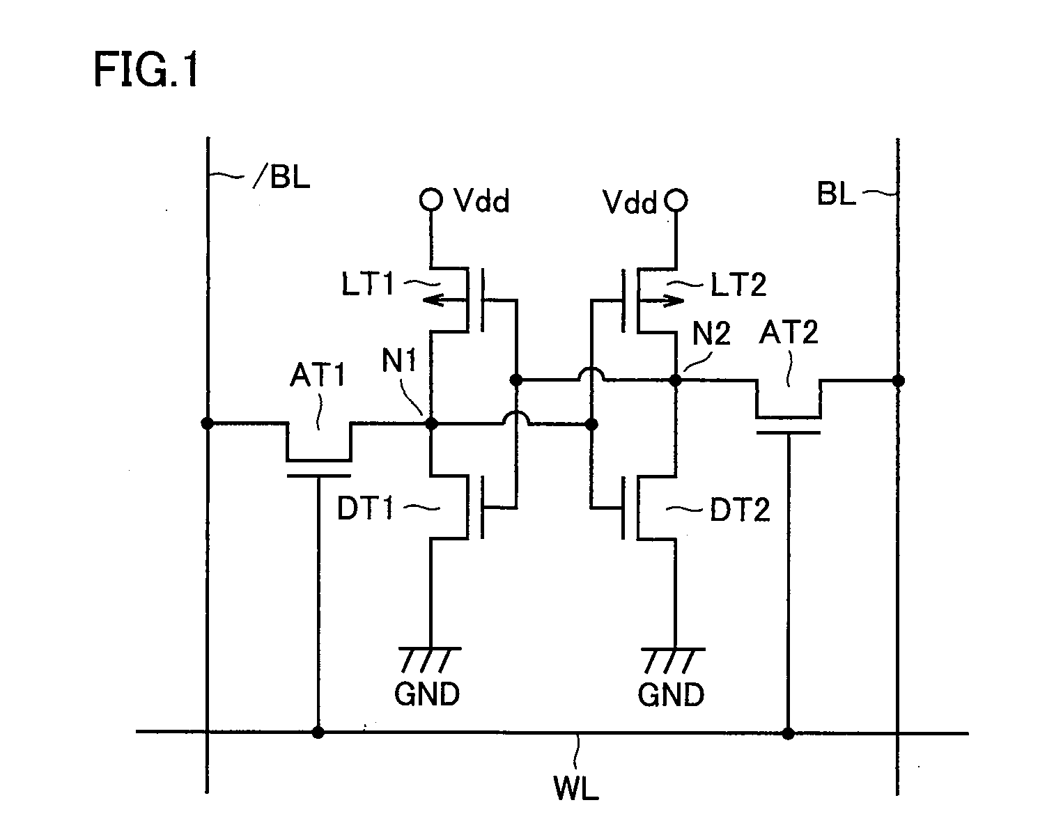
[0046]Referring to FIG. 1, an SRAM is a volatile semiconductor memory device, and a memory cell of the SRAM is a full CMOS (Complementary Metal Oxide Semiconductor) type memory cell.

[0047]In the SRAM, the memory cell is disposed in each of intersections of complementary data lines (bit lines) BL and / BL and word lines WL. Complementary data lines (bit lines) BL and / BL and word lines WL are disposed in a matrix shape. The memory cell includes a flip-flop circuit provided with a pair of inverter circuits and two access transistors AT1 and AT2. Cross-coupled two storage nodes N1 and N2 are formed to obtain a bistable state of (High, Low) or (Low, High) by the flip-flop circuit. The memory cell continuously retains the bistable state as long as a predetermined power supply voltage is applied to the memory cell.

[0048]Each of access transistors AT1 and AT2 includes an n-channel MOS transistor (hereinafter referred to as nMOS transistor). One of a source and a drain of access transistor A...

second embodiment

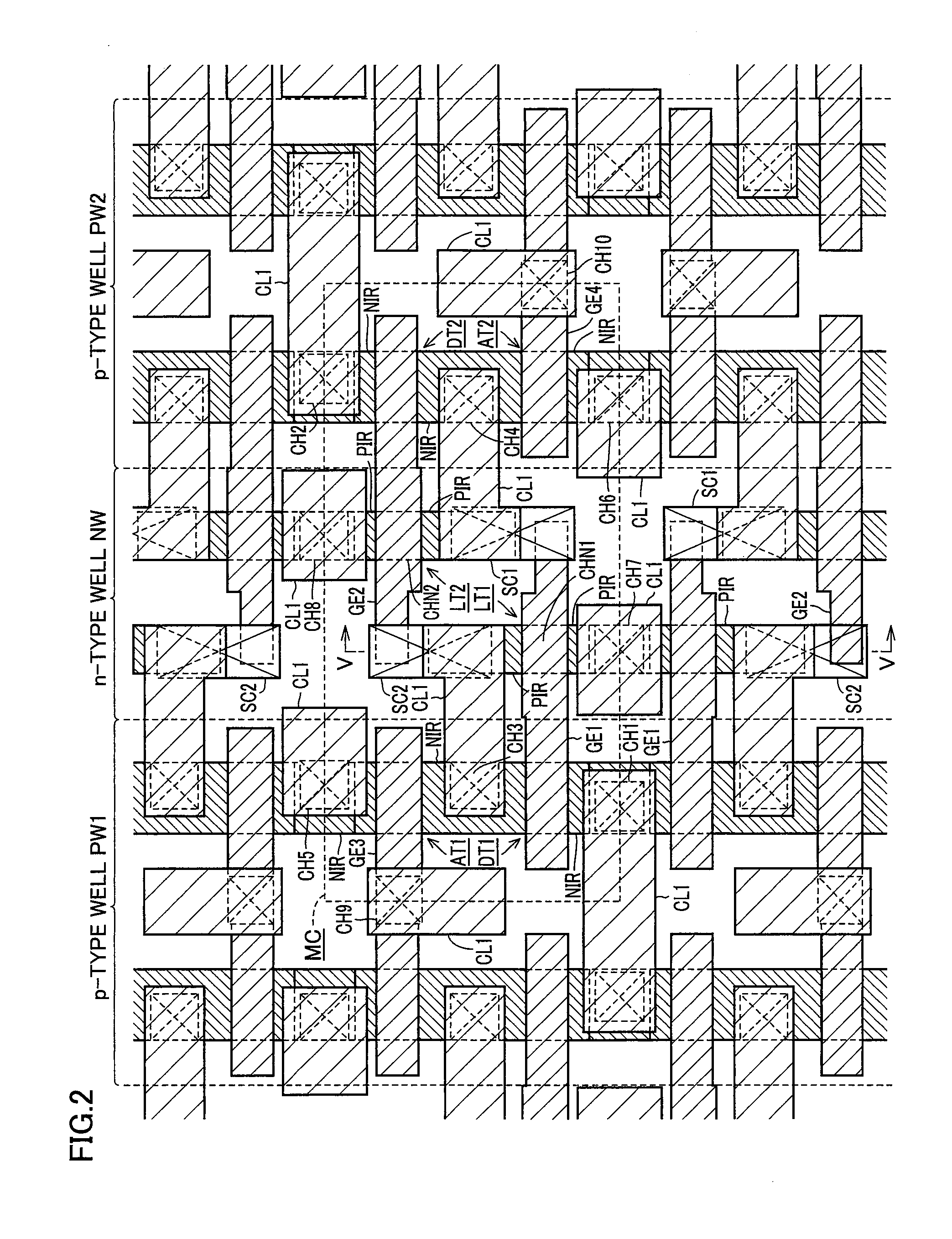
[0112]Referring to FIG. 21, a configuration of a second embodiment differs from the configuration of the first embodiment in that sidewall E2 is intersected with sidewall E1 while inclined relative to sidewall E1. Specifically, sidewall E2 is inclined so as to be retreated toward the side of sidewall E4 with respect to virtual extended line E1a of sidewall E1 as sidewall E2 is away from channel formation region CHN1, and sidewall E2 is intersected with virtual extended line E1a of sidewall E1 at an angle θ1.

[0113]In the planar view, the center line (line C2-C2) of line width D1 in the portion that shared contact hole SC1 of gate electrode layer GE1 reaches is shifted toward the side of sidewall E4 with respect to the center line (line C1 -C1) of line width D2 in the portion located on channel formation region CHN1 of gate electrode layer GE1. The center line (line C2-C2) of line width D1 is inclined relative to the center line (line C1-C1) of line width D2. Line width D1 and line wi...

third embodiment

[0124]In the first and second embodiments, sidewall E4 in the portion that shared contact hole SC1 (or SC2) of gate electrode layer GE1 (or GE2) reaches and sidewall E3 in the portion located on channel formation region CHN1 (or CHN2) of gate electrode layer GE1 (or GE2) are located on the same straight line. Moreover, the present invention can also be applied to the case in which sidewall E4 and sidewall E3 are located on different straight lines. Therefore, third and fourth embodiments will be described for the case in which sidewall E4 and sidewall E3 are located on different straight lines.

[0125]Referring to FIG. 23, a configuration of the third embodiment differs from the configuration of the first embodiment in that sidewall E4 is located on a straight line different from that of sidewall E3.

[0126]In the third embodiment, sidewall E4 in the portion that shared contact hole SC1 of gate electrode layer GE1 reaches is substantially extended in parallel with sidewall E3 in the por...


PUM

PropertyMeasurementUnit
distanceaaaaaaaaaa
widthaaaaaaaaaa
diameteraaaaaaaaaa

Abstract

Shared contact holes SC1 and SC2 reach both gate electrode layers GE1 and GE2 and a drain region PIR. In a planar view, a sidewall E2 of gate electrode layers GE1 and GE2 is shifted toward a side of a sidewall E4 from a virtual extended line E1a of the sidewall E1. In a planar view, a center line of a line width D1 in a portion that shared contact holes SC1 and SC2 of gate electrode layers GE1 and GE2 reach is located while shifted with respect to a center line of a line width D2 in a portion located on channel formation regions CHN1 and CHN2 of gate electrode layers GE1 and GE2. Therefore, a semiconductor device and a photomask that can suppress an opening defect of the shared contact hole are obtained.

Description

BACKGROUND OF THE INVENTION[0001]1. Field of the Invention[0002]The present invention relates to a semiconductor device and a photomask, particularly to a semiconductor device having a shared contact hole that reaches both a gate electrode layer and an impurity region and a photomask that is used in patterning of the gate electrode layer.[0003]2. Description of the Background Art[0004]For example, Japanese Patent Laying-Open Nos. 09-321152, 2004-273642, 2004-273972, and 2004-327796 disclose the semiconductor device having the shared contact hole that reaches both the gate electrode layer and the impurity region.[0005]Usually the shared contact hole has a tapered shape in section in which an opening diameter is decreased from an opening end toward a deep position. Therefore, when an etching film such as an insulator is etched to make the shared contact hole, an etching area of the etching film is reduced with the progress of etching. The reduction of the etching area obstructs the pr...

Claims


Application Information

Patent Timeline
Patent Type & Authority Applications(United States)
IPC IPC(8): H01L27/088G03F1/00H10B99/00H10B10/00
CPCH01L21/76895H01L27/0207H01L27/105H01L27/1052H01L27/1104H01L29/4238H01L27/11H10B10/00H10B10/12H10B99/00
Inventor TAKEUCHI, MASAHIKO
Owner RENESAS ELECTRONICS CORP
Features
  • R&D
  • Intellectual Property
  • Life Sciences
  • Materials
  • Tech Scout
  • Unparalleled Data Quality
  • Higher Quality Content
  • 60% Fewer Hallucinations
Learn More