

Display substrate, method of manufacturing the display substrate and display apparatus having the display substrate
- Summary
- Abstract
- Description
- Claims
- Application Information
AI Technical Summary
Benefits of technology
Problems solved by technology
Method used
Image

Examples
embodiment 1
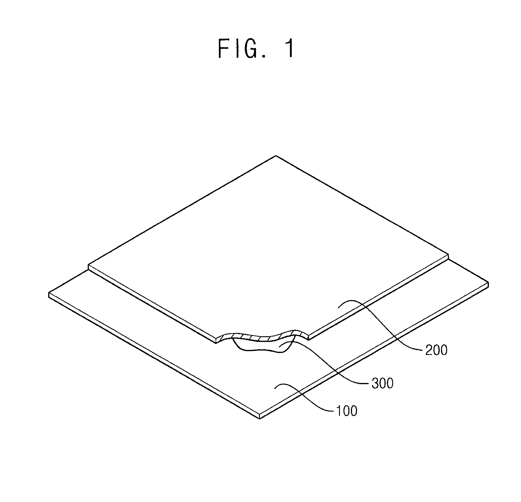
[0058]FIG. 1 is a perspective view illustrating a display apparatus in accordance with Embodiment 1 of the present invention.
[0059]Referring to FIG. 1, a display apparatus includes a first substrate 100, a second substrate 200 and a liquid crystal layer 300. The display apparatus displays an image using light.
[0060]The first substrate 100 may include a plurality of unit pixels arranged in a matrix form.
[0061]The second substrate 200 may be opposite to the first substrate 100. The second substrate 200 may include a plurality of color filters corresponding to the unit pixels and a common electrode formed on the entire surface of the second substrate 200 facing the first substrate 100. The color filters may include a red color filter, a green color filter and a blue color filter. In another embodiment of the present invention, the color filters may be formed on the first substrate 100.
[0062]The liquid crystal layer 300 is disposed between the first substrate 100 and the second substrat...
embodiment 2
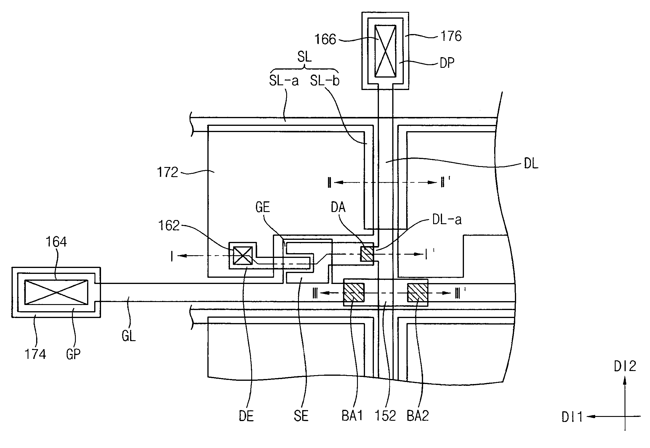
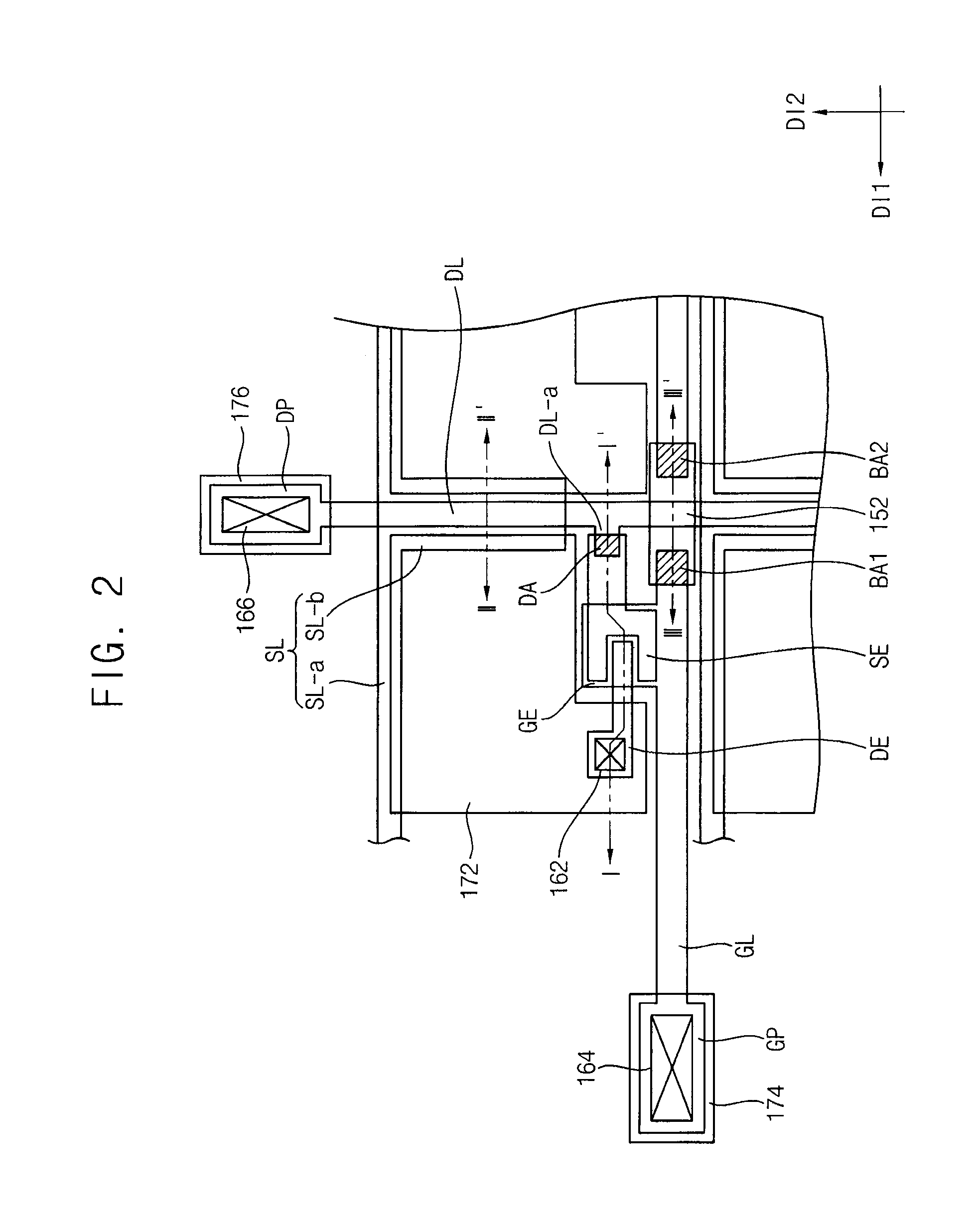
[0104]FIG. 5 is an enlarged plan view a first substrate employed in a display apparatus in accordance with Embodiment 2 of the present invention. FIG. 6A is a cross-sectional view taken along a line IV-IV′ shown in FIG. 5. FIG. 6B is a cross-sectional view taken along a line V-V′ shown in FIG. 5. FIG. 6C is a cross-sectional view taken along a line VI-VI′ shown in FIG. 5.
[0105]Referring to FIGS. 5 to 6C, a first substrate includes a base substrate 110, gate lines GL, data lines DL, line insulation patterns 132, space-filling insulation patterns 182, semiconductor patterns 142, TFTs, storage lines SL, bridge lines 152, a passivation layer 160, and pixel electrodes 172. Each of the TFTs includes a gate electrode GE, a source electrode SE and a drain electrode DE.
[0106]The base substrate 110 may have a plate shape. The base substrate 110 may include a transparent material. The base substrate 110 may include a display region displaying an image and a peripheral region surrounding the di...
embodiment 3
[0151]FIG. 8 is an enlarged plan view illustrating a portion of a first substrate employed in a display apparatus in accordance with Embodiment 3 of the present invention.
[0152]In Embodiment 3 of the present invention, components of the first substrate except for the gate lines, the data lines and the bridge lines are similar to or substantially the same as the components of the first substrate employed in the display apparatus in accordance with Embodiment 1 of the present invention. Thus, any repetitive explanation will be omitted.
[0153]Referring to FIG. 8, the gate lines GL are formed on the base substrate 110. The gate lines GL extend in a first direction DI1 and are arranged parallel to one another along a second direction different from the first direction DI2. For example, the second direction DI2 may be substantially perpendicular to the first direction DI1.
[0154]The data lines DL are also formed on the base substrate 110. The data lines DL are separated from the gate lines ...
PUM
 Abstract
Description
Claims
Application Information