Porous metal thin film, method for manufacturing the same, and capacitor

a technology of porous metal and thin film, which is applied in the direction of electrolytic capacitors, liquid electrolytic capacitors, electrolytic capacitors, etc., can solve the problems of surface asperities, surface becomes cloudy, and further roughening of the surface, so as to improve the capacitance of capacitors and enhance the performance of catalyst electrodes. , the effect of large surface area

Active Publication Date: 2009-07-09
KOBE STEEL LTD
View PDF45 Cites 7 Cited by
  • Summary
  • Abstract
  • Description
  • Claims
  • Application Information

AI Technical Summary

Benefits of technology

[0034]The porous metal thin film according to an aspect of the present invention has the specific film surface structure in which domains having an average diameter of 200 nm or more, and 500 nm or less and being formed through aggregation of a plurality of grains having an average grain diameter of 50 nm or more, and 160 nm or less are included, a gap of 5 nm or more, and 40 nm or less is present between a domain and another domain and, in addition, an area occupied by the domains relative to the total area of the film surface is 60% or mor

Problems solved by technology

However, in order to respond to demands for an increase in surface area which have been still intensified in recent years, further roughening of a surface is required.
In the case where an aluminum film is heat-formed, surface asperities are formed and the surface becomes cloudy.
It is believed that the aluminum

Method used


Image

  • Porous metal thin film, method for manufacturing the same, and capacitor
  • Porous metal thin film, method for manufacturing the same, and capacitor
  • Porous metal thin film, method for manufacturing the same, and capacitor

Examples


example 1

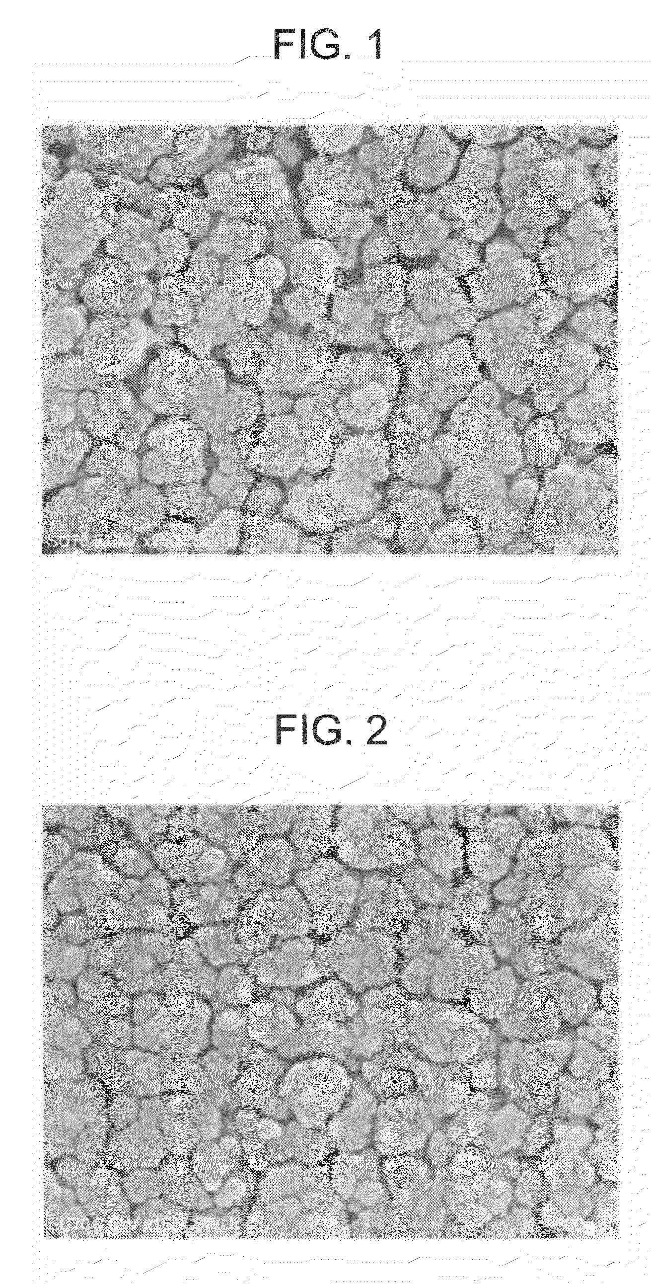
[0070]A porous aluminum thin film was formed by using a substrate composed of 1000 aluminum having a thickness of 1 mm and a diameter of 5.08 cm (2 inches) and by using a magnetron sputtering apparatus. A pure aluminum target having a purity of 4N was used as a sputtering target, an ultimate degree of vacuum was specified to be 1.2×10⁻⁶ Torr, and a 20% H2-80% Ar mixed gas was used as a film formation gas. DC discharge was conducted under the condition of a film formation gas pressure of 10 mTorr, a power feed of 10 W / cm2, and a distance between the substrate and the target of 60 mm. After film formation was conducted for 100 seconds, the film thickness was measured with a probe thickness gauge. The film thickness was 1,100 nm.

[0071]The surface of the resulting porous aluminum thin film was observed with a scanning electron microscope (SEM). FIG. 1 shows a photograph taken at 150,000-fold magnification. As shown in this photograph (FIG. 1), there are domains separated with black port...

example 2

[0075]A 1000 aluminum plate having a thickness of 1 mm and a diameter of 5.08 cm (2 inches) was subjected to an electrolysis treatment in 15% sulfuric acid solution at a DC current density of 150 A / m2 at a voltage of 15 V for 20 minutes, so that an anodized aluminum substrate including an anodized alumina film having a film thickness of 10 μm on a surface was prepared.

[0076]A porous aluminum thin film having a film thickness of 2,000 nm was formed as in Example 1 except that the resulting anodized aluminum substrate was used as the substrate, a 3% H2-97% Ar mixed gas was used as the film formation gas, and the power feed was specified to be 4 W / cm2.

[0077]The surface of the resulting porous aluminum thin film was observed with a scanning electron microscope (SEM). FIG. 2 shows a photograph taken at 150,000-fold magnification. As shown in this photograph (FIG. 2), there are domains separated with black portions on a surface of a porous aluminum thin film. The domain was formed through...

example 3

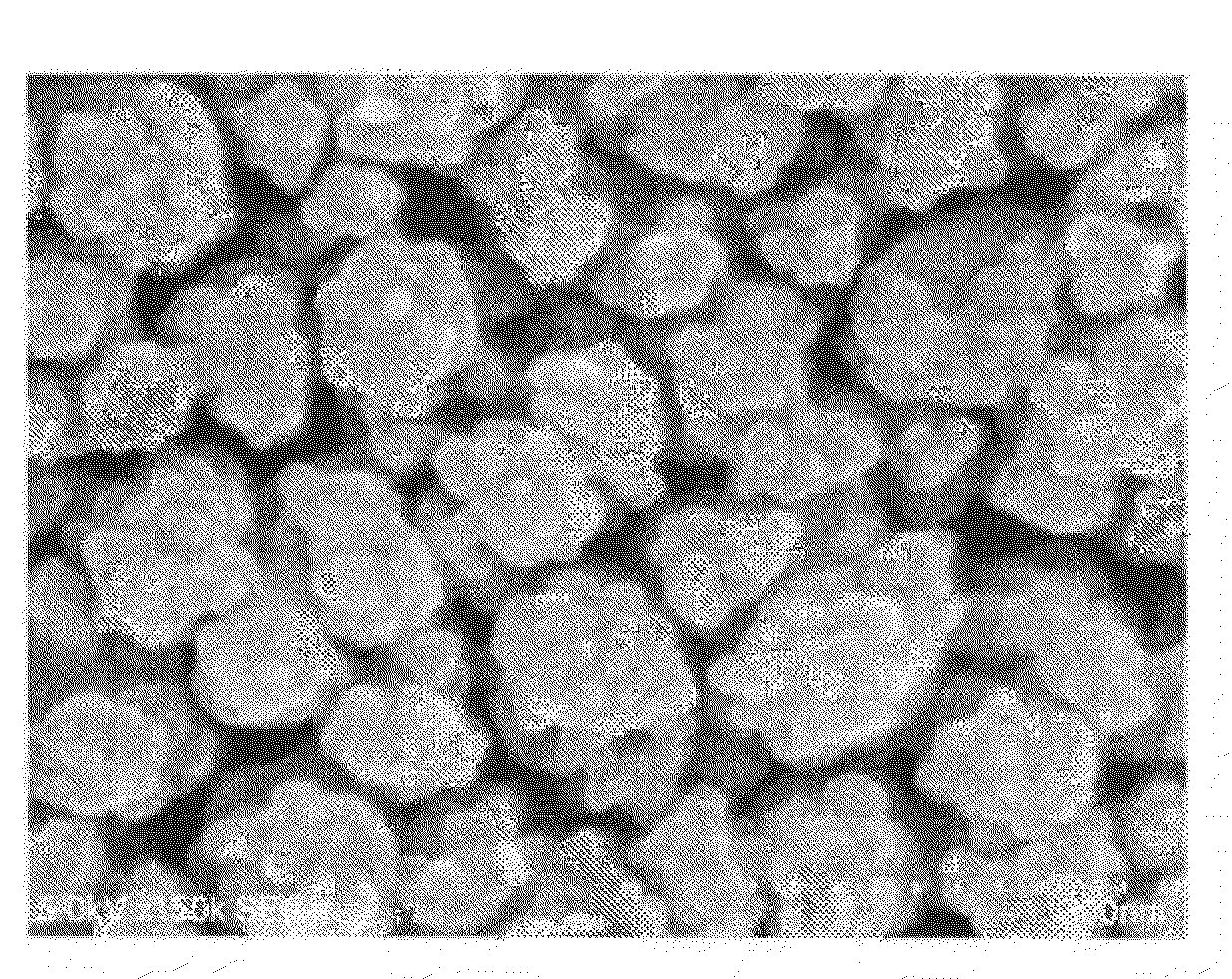
[0080]A porous aluminum thin film having a film thickness of 5,000 nm was formed on a substrate surface as in Example 1 except that a 10% H2-90% Ar mixed gas was used as the film formation gas, and the power feed was specified to be 4 W / cm2.

[0081]The surface of the resulting porous aluminum thin film was observed with a scanning electron microscope (SEM). FIG. 3 shows a photograph taken at 150,000-fold magnification. As shown in this photograph (FIG. 3), there are domains separated with black portions on a surface of a porous aluminum thin film. The domain was formed through aggregation of a plurality of spherical grains. Furthermore, finer spherical grain was not observed. This photograph was subjected to image analysis, so that the average diameter of domains and the average grain diameter of spherical grains were measured. As a result, the average grain diameter of spherical grains was 23 nm and the average diameter of domains formed through aggregation of spherical grains was 12...


PUM

PropertyMeasurementUnit
Fractionaaaaaaaaaa
Fractionaaaaaaaaaa
Fractionaaaaaaaaaa

Abstract

A porous metal thin film formed from aluminum has a film structure in which domains having an average diameter of 200 nm or more, and 500 nm or less and being formed through aggregation of a plurality of grains having an average grain diameter of 50 nm or more, and 160 nm or less are distributed discretely at an average distance of 5 nm or more, and 40 nm or less, wherein the area occupied by the above-described domains is 60% or more, and 90% or less in a cross-section in any direction of the porous metal thin film.

Description

BACKGROUND OF THE INVENTION[0001]1. Field of the Invention[0002]The present invention relates to a porous metal thin film having a large surface area, a method for manufacturing the same, and a capacitor.[0003]2. Description of the Related Art[0004]In recent years, surfaces of thin films have been roughened in order to improve the functions of the thin films. For example, for the purpose of improving the capacitance of an electrolytic capacitor, a surface of aluminum foil serving as an electrode material is roughened by a chemical conversion treatment so as to increase a surface area.[0005]In a catalyst field as well, platinum black and gold black produced by roughening surfaces of platinum and gold have been used as electrodes and catalysts for various chemical reactions. Furthermore, for example, carbon, ceramic, and metals have been used while surface areas thereof have been increased by surface roughening through conversion to a porous surface for the purpose of improving the fu...

Claims


Application Information

Patent Timeline
IPC IPC(8): H01G9/045B32B3/10B05D5/12
CPCC23C14/165H01G9/045H01G9/048Y10T428/256Y10T428/12438Y10T428/25Y10T29/417Y10T428/24413Y10T428/249953
Inventor MIZUNO, MASAO
Owner KOBE STEEL LTD
Why Eureka
Try Eureka