Storage cell having buffer circuit for driving the bitline

a buffer circuit and storage cell technology, applied in semiconductor devices, digital storage, instruments, etc., can solve the problems of affecting the robustness of write, and affecting the stability of the cell,

Active Publication Date: 2009-07-09
TEXAS INSTR INC
View PDF15 Cites 11 Cited by
  • Summary
  • Abstract
  • Description
  • Claims
  • Application Information

AI Technical Summary

Problems solved by technology

However, these characteristics generally contradict one another.
For example, low Vt and / or short gate lengths generally provide high Iread, but also result in high subthreshold leakage and poor cell stability.
Similarly, changes in the transistors (such as width, length, or threshold voltage) that improve the cell stability during a Read generally degrade the robustness of the Write.
However, this separation of read functionality and write functionality of the conventional 8T is not effective in conventional SRAM architectures where words are interleaved in a row.
Cells that are in a selected row but not a selected column (half selected cells) are subject to upset during a Write cycle.
Nevertheless, there will generally still be a strong differential between read current and leakage current.
An alternative is to lower the VDD for the array, shown as VDDAR145, but this can cause a greater degradation of SNM, and also reduce Iread.
This arrangement generally improves SNM but can degrade the robustness of the Write.
However, in this differential Write arrangement, the improved dynamic stability from the buffer circuit on the single BL described above would not generally be adequate stability protection for the half selected cells in a Write operation.

Method used


Image

  • Storage cell having buffer circuit for driving the bitline
  • Storage cell having buffer circuit for driving the bitline
  • Storage cell having buffer circuit for driving the bitline

Examples


first embodiment

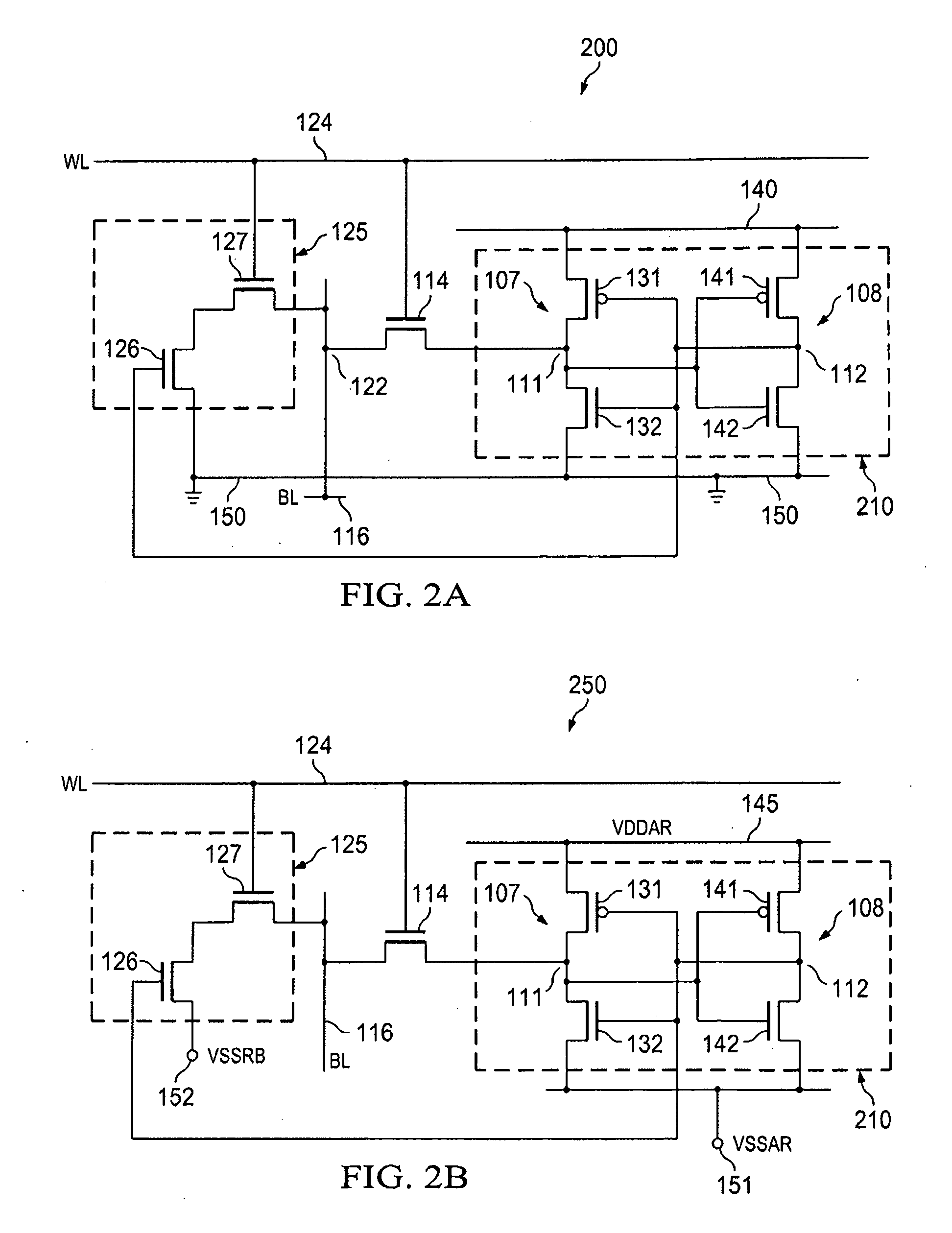
[0047]FIG. 2D is a timing diagram showing the operation of a memory cell, such as cell 250, through a Read cycle, a Write cycle and a Standby cycle, in a first embodiment that realizes a delayed boosted WL level during a Write operation. During the Write operation shown, the WL 124 initially rises to VDD, then after a delay sufficient for the establishment of a stable voltage on the BL's 116 of the half addressed cells, WL 124 rises to a level above VDD.

second embodiment

[0048]FIG. 2E is a timing diagram showing the operation of a memory cell, such as cell 250, according to an embodiment of the invention through a Read cycle, a Write cycle and a Standby cycle, in a second embodiment that realizes a delayed boosted WL level during a Write operation. During the Write operation shown the WL 124 initially rises to a level below VDD, then after a delay sufficient for the establishment of a stable voltage on the BL's 116 of the half addressed cells, WL 124 rises to VDD.

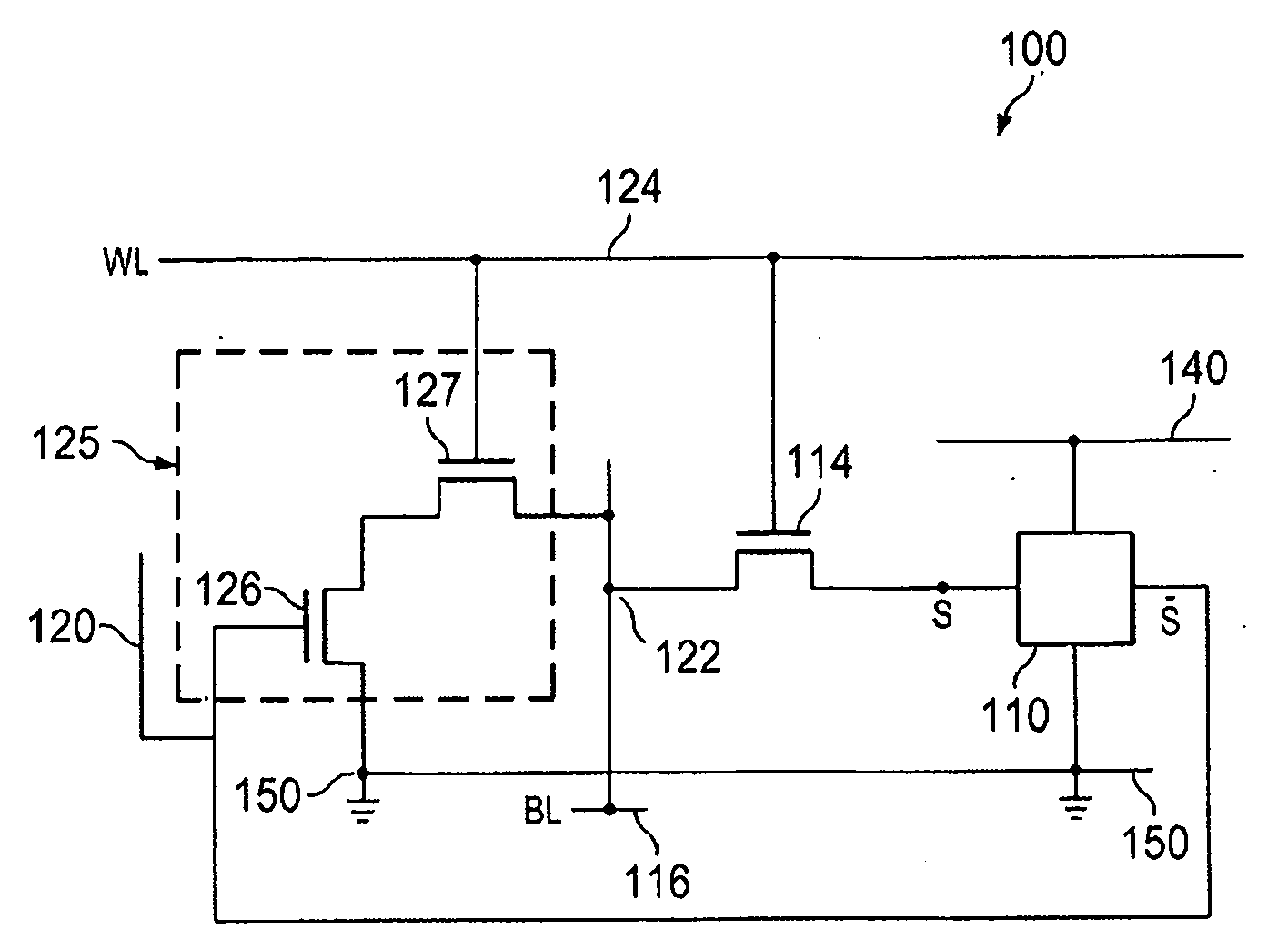
[0049]FIG. 3A is a schematic of a 7T memory cell 300 with a single Read / Write BL 116, with Read / WL 124, in an alternate topology for generally improved stability, according to another embodiment of the invention. Read / Write BL 116 is now connected to a source / drain of pass gate 127. The other source / drain of pass gate 127 is now connected to the drain of driver 126 and to a source / drain of pass gate 114. For cell 300, the first storage node 111 of core storage element 210 is separated from ...


PUM


Abstract

An integrated circuit includes a memory array including a plurality of memory cells, the memory cells include a core storage element having at least a first storage node (S) and a complementary second storage node (S-bar), and a first pass gate ) coupled to the first storage node (S). A single bitline (BL) is coupled to a node in a source drain path of the first pass gate. The BL is for Reading data from and Writing data to the first storage node (S). A buffer circuit includes a second pass gate and a driver transistor, wherein the second pass gate is coupled between the driver transistor and the source drain path of the first pass gate. A gate of the driver transistor is coupled to the second storage node (S-bar). At least one wordline (WL) is coupled to the first pass gate and the second pass gate.

Description

CROSS REFERENCE TO RELATED APPLICATION[0001]This application claims the benefit of Provisional Application Ser. No. 61 / 019,024 entitled “10T SRAM Cell with 1 WL and 2 BL's (BL and BL_)”, filed Jan. 4, 2008, Provisional Application Ser. No. 61 / 019,028 entitled: “7T SRAM CELL WITH 1 WL AND 1 BL”, filed Jan. 4, 2008, and Provisional Application Ser. No. 61 / 019,020 entitled: “METHOD FOR ACCELERATING MONTE CARLO EVALUATIONS, AND CIRCUITS DESIGNED BY THIS METHOD”, filed Jan. 4, 2008 which are all herein incorporated by reference in their entireties.FIELD OF INVENTION[0002]The present invention relates generally to semiconductor memory devices and more particularly to integrated circuits having memory cells that include read buffer circuitry.BACKGROUND[0003]The basic CMOS 6T SRAM cell generally includes two n-type or n-channel (NMOS) pull-down or drive transistors and two p-type (PMOS) pull-up or load transistors in a cross-coupled inverter configuration, with two additional NMOS select or...

Claims


Application Information

Patent Timeline
Patent Type & Authority Applications(United States)
IPC IPC(8): G11C11/00G11C7/00
CPCH01L27/0207H01L27/1104H01L27/11H10B10/00H10B10/12
Inventor HOUSTON, THEODORE WARREN
Owner TEXAS INSTR INC
Why Eureka
Try Eureka