Dual node access storage cell having buffer circuits

a buffer circuit and storage cell technology, applied in the field of integrated circuits having dual node access memory cells, can solve the problems of affecting the robustness of write, and affecting the stability of the cell,

Active Publication Date: 2009-07-09
TEXAS INSTR INC
View PDF7 Cites 23 Cited by
  • Summary
  • Abstract
  • Description
  • Claims
  • Application Information

AI Technical Summary

Problems solved by technology

However, these characteristics generally contradict one another.
For example, low Vt and/or short gate lengths generally provide high Iread, but also result in high subthreshold leakage and poor cell stability.
Similarly, changes in the transistors (such as width, length, or threshold voltage) that improve the stability during a READ generally degrades the robustness of the WRITE.
However, this separation

Method used


Image

  • Dual node access storage cell having buffer circuits
  • Dual node access storage cell having buffer circuits
  • Dual node access storage cell having buffer circuits

Examples


first embodiment

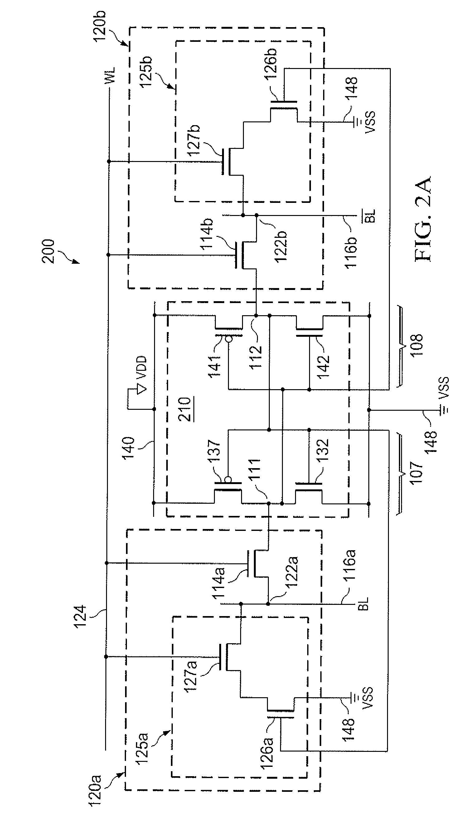
[0050]In one embodiment of the invention, a more robust WRITE operation can be achieved by using two or more different voltage levels on the WL during a WRITE operation. This is conceptually illustrated in FIG. 2F. FIG. 2F is a timing diagram showing the operation of a memory cell, such as cells 200 or 250, through a READ cycle, a WRITE cycle and a Standby cycle, in a first embodiment that realizes a delayed boosted WL level during a WRITE operation. As shown in FIG. 2F, during a WRITE operation the READ / WRITE WL 124 shown in FIGS. 2A and 2B can transition initially to a first voltage level and later during the WRITE operation transition to a second voltage level that is a higher as compared to the first voltage level. Boosting the WL voltage in the WRITE cycle after some delay time allows an initial establishment of a voltage on the BL's of the half addressed cells which can improve the stability of the half selected cells while the delayed boost of the WL can lead to a more robust...

second embodiment

[0051]FIG. 2G is a timing diagram showing the operation of a memory cell according to an embodiment of the invention through a READ cycle, a WRITE cycle and a Standby cycle, in a second embodiment that realizes a delayed boosted WL, level during a WRITE operation. During the WRITE operation shown the WL 124 initially rises to a level below VDD, then after a delay sufficient for the establishment of a stable voltage on the BL's of the half addressed cells, WL, rises to VDD.

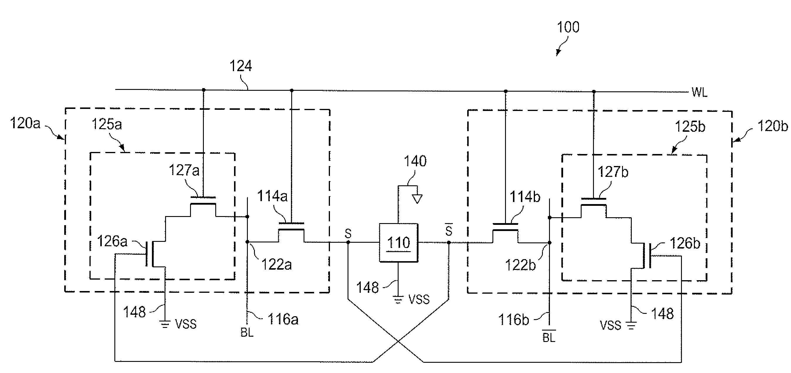
[0052]FIG. 3A is a schematic of a 10 T cell 300 with a common READ / WRITE BL's (BL 116a and BL116b) with common READ / WRITE WL 124, in an alternate topology for generally improved stability, according to another embodiment of the invention. As shown in FIG. 3A BL 116a and BL116b are now connected to the drains of buffer pass transistors 127a and 127b, respectively. The source of buffer pass transistors 127a and 127b are now connected to the drain of buffer driver transistors 126a and 126b, respectively. For cell 300,...


PUM


Abstract

An integrated circuit includes an array of memory cells, each including a core storage element with first and second complementary storage nodes and first and second cell pass transistors coupled to the first and second storage nodes, respectively. In the cell, a first bitline (BL) is coupled to a first BL node in a source drain path of the first cell pass transistor, and a second BL is coupled to a second BL node in a source drain path of the second cell pass transistor. Each of the memory cells also includes a first buffer circuit comprising a first buffer pass transistor and a first driver transistor coupled to the source drain path of the first cell pass transistor, where the first buffer pass transistor is between the first BL node and the first driver transistor. The memory cells also include a second buffer circuit comprising a second buffer pass transistor and a second driver transistor coupled to a source drain path of the second cell pass transistor, where the second buffer pass transistor is between the second BL node and the second driver transistor. The gates of the first and second driver transistors are coupled to the second and first storage nodes, respectively. The cells include at least a first wordline coupled to the first and second cell pass transistors and the first and second buffer pass transistors.

Description

CROSS REFERENCE TO RELATED APPLICATION[0001]This application claims the benefit of Provisional Application Ser. No. 61 / 019,024 entitled “10 T SEAM Cell with 1 WL and 2 BL's (BL and BL_)”, filed Jan. 4, 2008, Provisional Application Ser. No. 61 / 019,028 entitled: “7 T SRAM CELL WITH 1 WL AND 1 BL”, filed Jan. 4, 2008, and Provisional Application Ser. No. 61 / 019,020 entitled: “METHOD FOR ACCELERATING MONTE CARLO EVALUATIONS, AND CIRCUITS DESIGNED BY THIS METHOD”, filed Jan. 4, 2008 which are all herein incorporated by reference in their entireties.FIELD OF INVENTION[0002]The present invention relates generally to semiconductor memory devices and more particularly integrated circuits having dual node access memory cells that include buffer circuitry storage element of the memory cells.BACKGROUND[0003]The basic CMOS 6 T SRAM cell generally includes two n-type or n-channel (NMOS) pull-down or drive transistors and two p-type (PMOS) pull-up or load transistors in a cross-coupled inverter c...

Claims


Application Information

Patent Timeline
IPC IPC(8): G11C11/00G11C7/00
CPCH01L27/0207H01L27/1104H01L27/11H10B10/00H10B10/12
Inventor HOUSTON, THEODORE WARREN
Owner TEXAS INSTR INC
Why Eureka
Try Eureka