Semiconductor device

a technology of semiconductors and devices, applied in the direction of semiconductor devices, electrical appliances, transistors, etc., can solve the problems of large snapback phenomenon, reduced lifetime, increased defect layer, etc., to reduce the variation of low saturation voltage vce, stabilize the loss of a switching characteristic, and improve the robustness against the destruction of an igbt module in an individual operation.

Active Publication Date: 2009-07-23
MITSUBISHI ELECTRIC CORP
View PDF9 Cites 23 Cited by
  • Summary
  • Abstract
  • Description
  • Claims
  • Application Information

AI Technical Summary

Benefits of technology

[0016]Furthermore, there can be provided a 3.3 KV-Planaer-IGBT having a semiconductor substrate having a back surface that has a pn structure containing an impurity controlled in concentration and diffused to a depth, as controlled, and is exposed to protons in a controlled amount to eliminate snapback phenomenon of low saturation voltage Vce (sat) for operation at a low temperature of −55° C. to reduce variation in low saturation voltage Vce (sat) and stabilize a loss of a switching characteristic.
[0017]Furthermore, the robustness against destruction of an IGBT module in an individual operation can also be improved. A semiconductor substrate can thus have a back surface that has a p type collector layer and an n type buffer layer having their respective impurities controlled in concentration and depth and is exposed to protons for a donor layer in a controlled amount to provide a high withstand voltage power device IGBT as a product ranging from high to low speed applications.

Problems solved by technology

When an n− type semiconductor substrate is exposed to a large quantity of protons, it has an increased defect layer.
This results in a reduced lifetime.
If the product is small, a large snapback phenomenon manifests.

Method used


Image

  • Semiconductor device
  • Semiconductor device
  • Semiconductor device

Examples


first embodiment

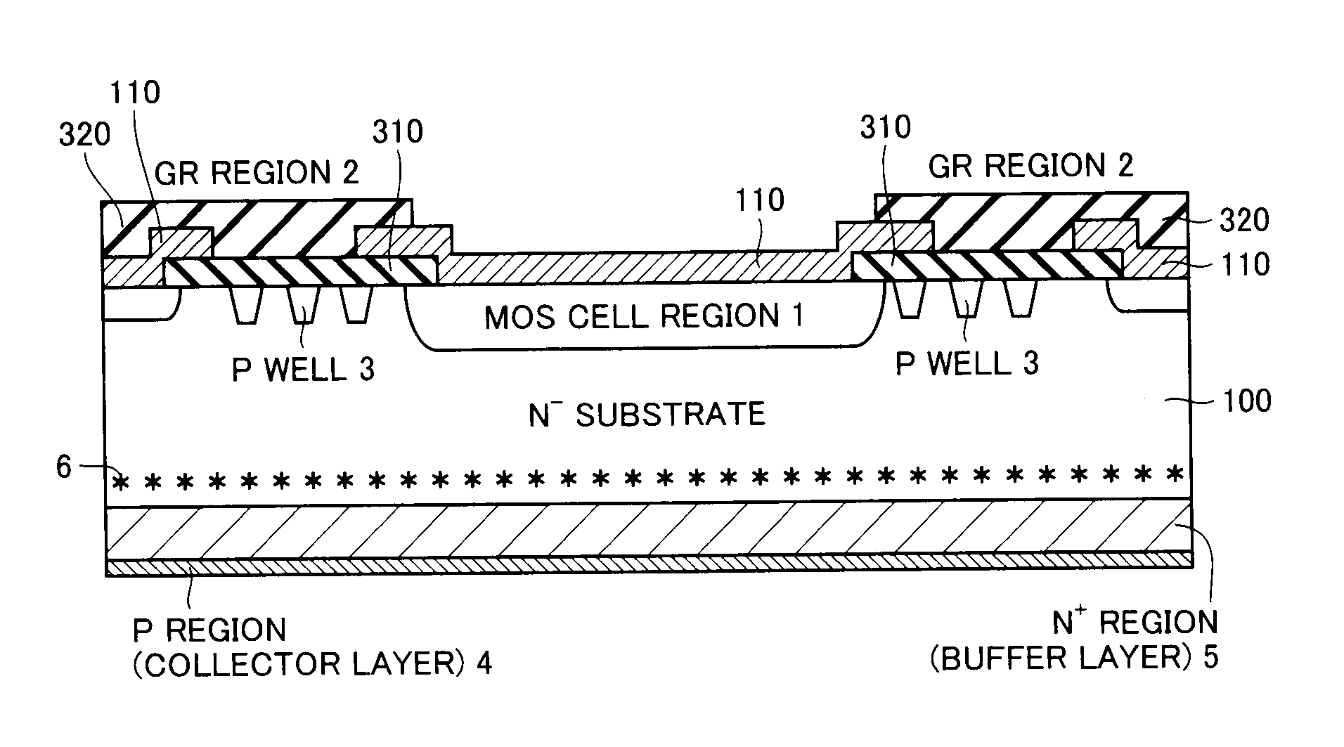
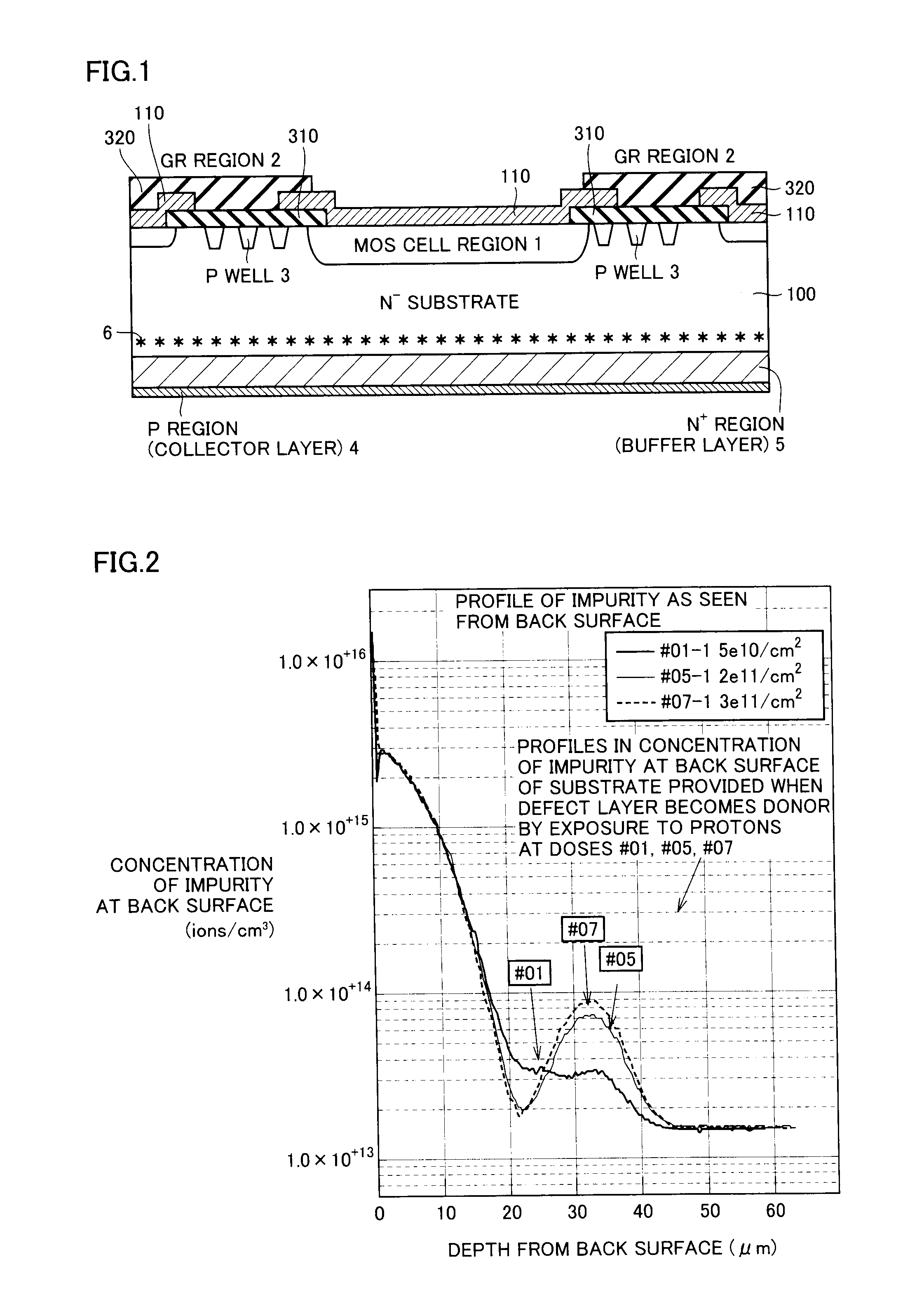
[0027]With reference to FIG. 1, the present embodiment provides a high withstand voltage power device IGBT, as will be described hereinafter.

[0028]An n− type semiconductor substrate 100 has a back surface provided with a p type collector layer 4 and an n+ type buffer layer 5. N− type semiconductor substrate 100 has a front surface provided at a center with a MOS cell region 1. MOS cell region 1 underlies gate electrode 110 with a gate insulation film (not shown) posed therebetween.

[0029]Furthermore, MOS cell region 1 is surrounded by a guard ring region 2. More specifically, n− type semiconductor substrate 100 has a front surface provided with a plurality of p type wells 3 that configure a guard ring annularly to surround MOS cell region 1. P type well 3 underlies a field oxide film 310 and an interlayer insulation film 320.

[0030]Maintaining a high withstand voltage power device IGBT's characteristic in withstand voltage requires optimizing n− type semiconductor substrate 100 in thi...


PUM


Abstract

A semiconductor device having the present high withstand voltage power device IGBT has at a back surface a p collector layer with boron injected in an amount of approximately 3×10¹³/cm2 with an energy of approximately 50 KeV to a depth of approximately 0.5 μm, and an n+ buffer layer with phosphorus injected in an amount of approximately 3×10¹²/cm2 with an energy of 120 KeV to a depth of approximately 20 μm. To control lifetime, a semiconductor substrate is exposed to protons at the back surface. Optimally, it is exposed to protons at a dose of approximately 1×10¹¹/cm2 to a depth of approximately 32 μm as measured from the back surface. Thus snapback phenomenon can be eliminated and an improved low saturation voltage (Vce (sat))-offset voltage (Eoff) tradeoff can be achieved.

Description

BACKGROUND OF THE INVENTION[0001]1. Field of the Invention[0002]The present invention relates generally to semiconductor devices and particularly to structures of semiconductor devices that allows a high withstand voltage power device insulated gate bipolar transistor (IGBT) to have an improved electrical characteristic by shallowing a back surface structure and exposing it to protons in an optimized amount to improve low saturation voltage (Vce (sat))-offset voltage (Eoff) tradeoff to allow a semiconductor device having the high withstand voltage power device IGBT for electric power to have a stabilized characteristic and maintain robustness against destruction.[0003]2. Description of the Background Art[0004]For electric railroad applications, inverters and converters are controlled by employing semiconductor devices for electric power that are implemented as IGBT module. For electric railroad applications, high withstand voltage IGBTs mainly of 3.3 KV and 6.5 KV are employed.[0005...

Claims


Application Information

Patent Timeline
Patent Type & Authority Applications(United States)
IPC IPC(8): H01L29/739
CPCH01L29/0619H01L29/0834Y10S257/901H01L29/66333H01L29/7395H01L29/36H01L29/70H01L29/73
Inventor HISAMOTO, YOSHIAKI
Owner MITSUBISHI ELECTRIC CORP
Why Eureka
Try Eureka