Transistor voltage-controlled oscillator

a voltage-controlled oscillator and transistor technology, applied in the direction of oscillator, pulse generator, pulse technique, etc., can solve the problems of low q-factor, power consumption of voltage-controlled oscillating circuit, and large reduction of die size, so as to reduce the parasitic capacitance, reduce power consumption, and increase the q-factor of the inductor

Inactive Publication Date: 2009-07-23
NAT TAIWAN UNIV
View PDF8 Cites 21 Cited by
  • Summary
  • Abstract
  • Description
  • Claims
  • Application Information

AI Technical Summary

Benefits of technology

[0012]In view of the above disadvantages of the conventional technique, it is a primary objective of the present invention to provide a transistor voltage-controlled oscillator that allows an integration of multiple inductors into a single chip, thereby reducing the die size significantly.
[0013]Another objective of the invention is to provide a transistor voltage-controlled oscillator that allows integrating inductors into the silicon chip during the chip process, thereby lowering the power consumption due to parasitic resistance of the silicon substrate, such that the problem of low Q-factor is avoided.
[0015]In comparison to the conventional technique, the transistor voltage-controlled oscillator in the present invention includes a first transformer inductor having a first induction coil and a second induction coil, further the first induction coil is connected to the first drain terminal, the second induction coil is connected to the first source terminal; and a second transformer inductor including a third induction coil and a fourth induction coil, further the third induction coil is connected to the second drain terminal, the fourth induction coil is connected to the second source terminal. The two above-mentioned transformer inductors are used as the coupling inductors in the cross-coupled LC-tank transistor voltage-controlled oscillating circuit thus, the area taken up by the inductor of the transistor voltage-controlled oscillator can be greatly reduced. As reducing the inductor area lowers the parasitic capacitance present between the inductor and the silicon substrate, a significant reduction in the power consumption can be achieved, which in turn increases the Q-factor of the inductor.

Problems solved by technology

Also, as a voltage-controlled oscillator often comprises quite a number of capacitors, inductors, transistors and other active or passive components, therefore the voltage-controlled oscillating circuit has always been the part in the wireless RF circuit that takes up the largest area and consumes the most power.
Firstly, power consumption of the voltage-controlled oscillating circuit is discussed.
As described above, even though integrating chip inductor on the silicon substrate leads to substrate parasitic resistance that attenuates the signal, thereby causing the problem of low Q-factor, most researches still focus on integrating inductors into the chip.
Hence, it has become an urgent issue to designers in the voltage-controlled oscillator to devise a way to design a voltage-controlled oscillating circuit that not only enables integration of multiple inductors into a single chip such that the die size is greatly reduced but also lowers the energy consumed by the parasitic resistance present in the silicon substrate during the process of integrating inductors into a silicon chip, thereby avoiding the problem of low Q-factor.

Method used


Image

  • Transistor voltage-controlled oscillator
  • Transistor voltage-controlled oscillator
  • Transistor voltage-controlled oscillator

Examples


first embodiment

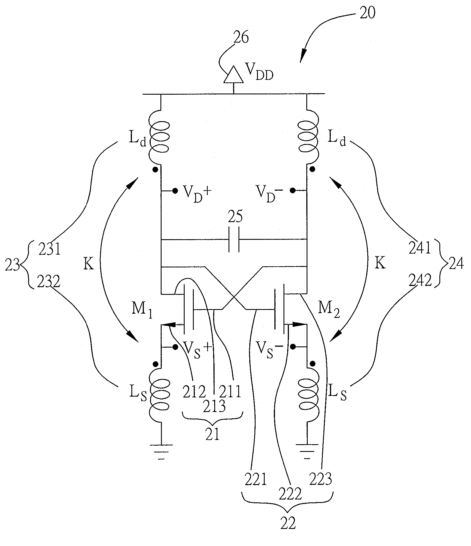
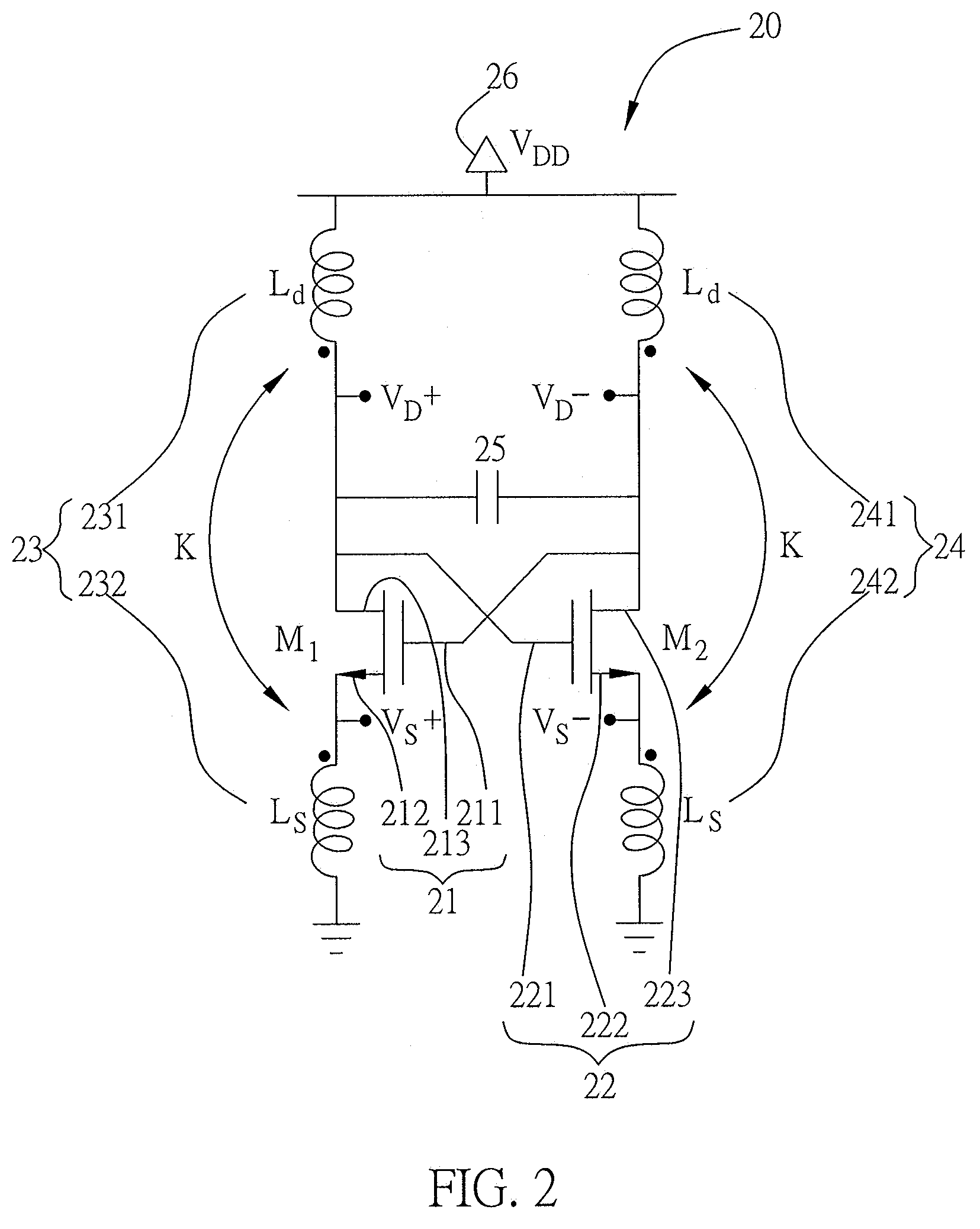
[0024]Referring to FIG. 2, a circuit diagram of a transistor voltage-controlled oscillator in the present invention is illustrated. The oscillator is a cross-coupled LC-tank transistor voltage-controlled oscillating circuit 20 having a first transistor 21 with a first gate terminal 211, a first source terminal 212 and a first drain terminal 213; a second transistor 22 with a second gate terminal 221, a second source terminal 222 and a second drain terminal 223, wherein the first gate terminal 211 is coupled to the second drain terminal 223 and the second gate terminal 221 is coupled to the first drain terminal 213, forming a cross-coupled transistor structure; a first transformer inductor 23, wherein the inductor is a coupling inductor in the cross-coupled LC-tank voltage-controlled oscillating circuit 20, and the first transformer inductor 23 includes a first induction coil 231 and a second induction coil 232, further the first induction coil 231 is connected to the first drain ter...

second embodiment

[0028]Referring to FIG. 4, a circuit diagram of a transistor voltage-controlled oscillator in the second embodiment is illustrated. The difference between the second embodiment and the first embodiment is that an NMOS transistor variable capacitor set 250 replaces the capacitor set 25; the NMOS transistor variable capacitor set 250 includes a third transistor 251 and a fourth transistor 252.

[0029]Also, the third transistor 251 includes a third gate terminal 2511, a third source terminal 2512, a third drain terminal 2513 and a third substrate 2514, and the fourth transistor 252 includes a fourth gate terminal 2521, a fourth source terminal 2522, a fourth drain terminal 2523 and a fourth substrate 2524. The third source terminal 2512 is coupled to the third drain terminal 2513, the fourth source terminal 2522 is coupled to the fourth drain terminal 2523. Furthermore the third substrate 2514 is coupled to the first drain terminal 213, and the fourth substrate 2524 is coupled to the sec...

third embodiment

[0030]Referring to FIG. 5, a circuit diagram of a transistor voltage-controlled oscillator of the present invention in the third embodiment is illustrated. The difference between the third embodiment and the second embodiment is that the transistor voltage-controlled oscillator in the third embodiment includes two extra sets of output buffer amplifiers 281 and 282 which serve the purpose of stabilizing the output signals of the transistor voltage-controlled oscillator and increasing the output signal swing.


PUM


Abstract

A transistor voltage-controlled oscillator includes a cross-coupled LC-tank transistor voltage-controlled oscillating circuit composed of two transistors, a capacitor set, and a first transformer inductor having a first inductor coil and a second inductor coil coupled to the first inductor coil; and a second transformer inductor having a third inductor coil and a fourth inductor coil coupled to the third inductor coil. The first transformer inductor and the second transformer inductor are both used as a coupling inductor for the cross-coupled LC-tank transistor voltage-controlled oscillating circuit. As a result, the inductor area of the transistor voltage-controlled oscillator is greatly reduced and the parasitic capacitance between the inductors and the silicon substrate is reduced accordingly such that the power consumption is greatly reduced and the quality factor of the inductor is increased.

Description

BACKGROUND OF THE INVENTION[0001]1. Field of the Invention[0002]The invention relates to a voltage-controlled oscillator, and more specifically, to a transistor voltage-controlled oscillator.[0003]2. Prior Art[0004]Design of a voltage-controlled oscillator has always been the design focus in the field of wireless communications circuit design. In the wireless RF circuit, the voltage-controlled oscillator plays an extremely crucial role in the modulation / demodulation process of the RF front-end circuit. Also, as a voltage-controlled oscillator often comprises quite a number of capacitors, inductors, transistors and other active or passive components, therefore the voltage-controlled oscillating circuit has always been the part in the wireless RF circuit that takes up the largest area and consumes the most power.[0005]FIG. 1 depicts a conventional cross-coupled LC-tank transistor voltage-controlled oscillator. The voltage-controlled oscillator consists of a pair of cross-coupled trans...

Claims


Application Information

Patent Timeline
Patent Type & Authority Applications(United States)
IPC IPC(8): H03B5/24
CPCH03B5/1228H03B5/1253H03B5/1296H03B5/1212
Inventor DENG, PING-YUANKIANG, JEAN-FU
Owner NAT TAIWAN UNIV
Why Eureka
Try Eureka