Electronic element, variable capacitor, micro switch, method for driving micro switch, and MEMS type electronic element

a technology of electronic elements and micro switches, applied in the direction of variable capacitors, instruments, and semiconductor/solid-state device details, etc., can solve the problems of inability to stably balance spring force and electrostatic force with each other, small q value of varactors, and various inconveniences, so as to reduce driving voltage and sacrifice reliability

Active Publication Date: 2009-07-30
NIKON CORP
View PDF15 Cites 13 Cited by
  • Summary
  • Abstract
  • Description
  • Claims
  • Application Information

AI Technical Summary

Benefits of technology

[0046]According to the present invention as defined above, it is possible to provide the micro switch which makes it possible to decrease the driving voltage without causing any special inconvenience or problem which would be otherwise caused such that the signal pass characteristic is sacrificed and/or the reliability is sacrifice

Problems solved by technology

However, the Q value of the varactor is small, and various inconveniences arise.
In the variable capacitor disclosed in “A micromachined variable capacitor for monolithic low-noise VCOs”, however, when the voltage applied between the both electrodes is increased and when the spacing distance between the both electrodes becomes narrower than the spacing distance of about ⅓ of the initial spacing distance, then the spring force and the electrostatic force cannot be stably balanced with each other.
In the high frequency band, the transmission loss, which results from the low Q of the switch which is the conventional semiconductor

Method used


Image

  • Electronic element, variable capacitor, micro switch, method for driving micro switch, and MEMS type electronic element
  • Electronic element, variable capacitor, micro switch, method for driving micro switch, and MEMS type electronic element
  • Electronic element, variable capacitor, micro switch, method for driving micro switch, and MEMS type electronic element

Examples


first embodiment

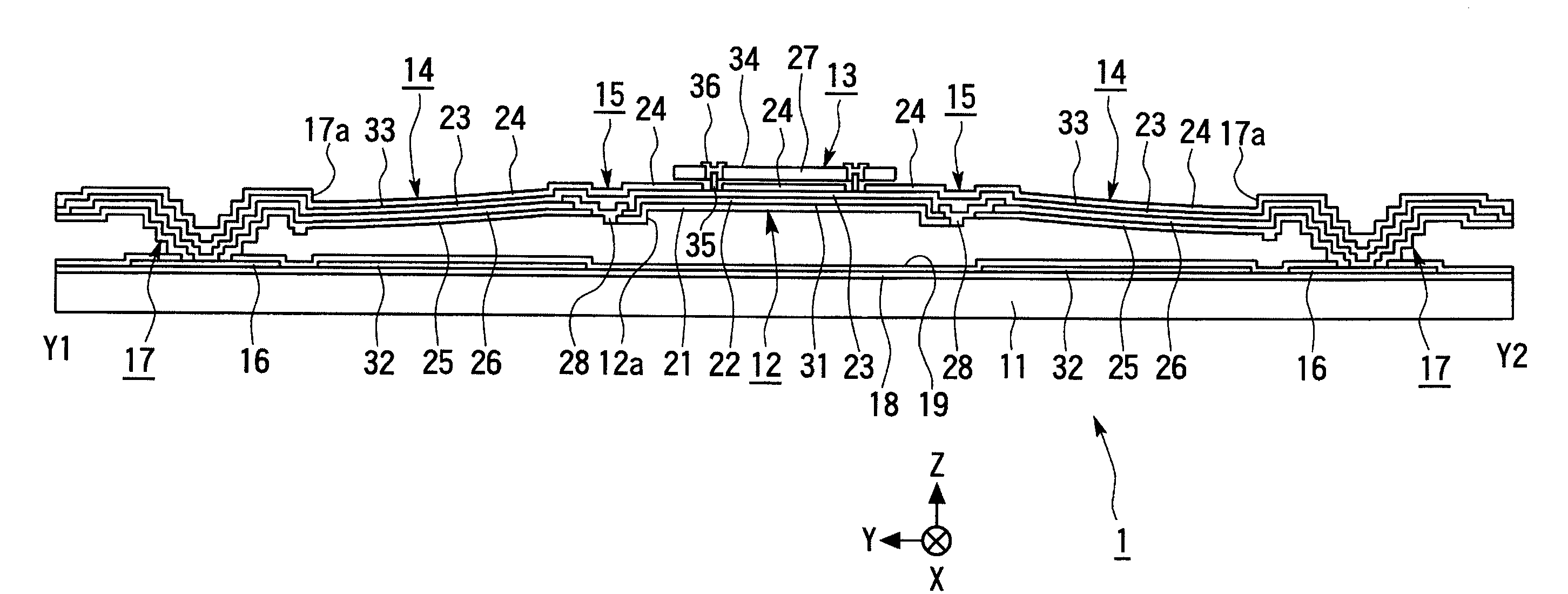
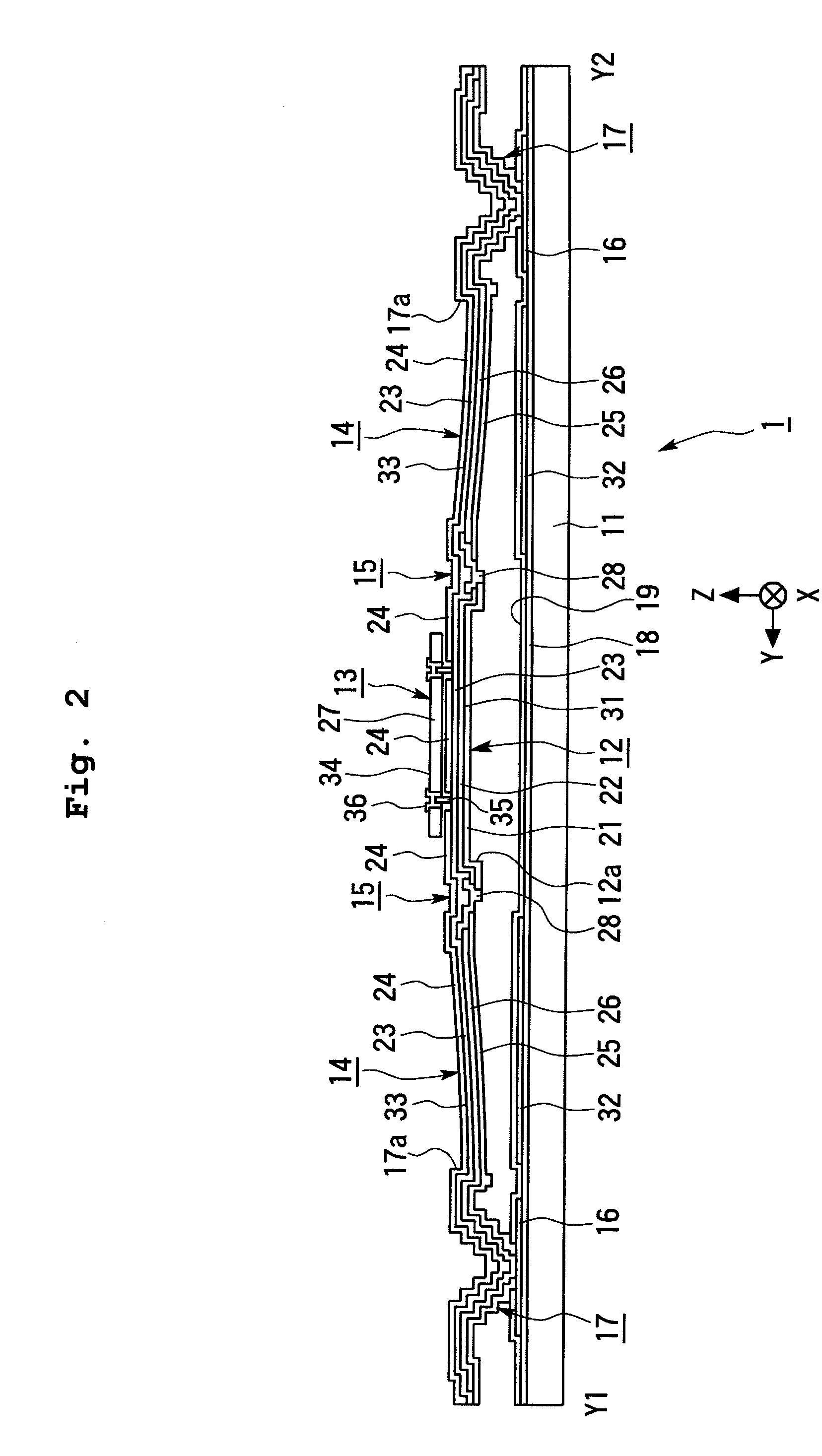
[0081]FIG. 1 shows a schematic plan view of a general construction of a variable capacitor 1 according to the first embodiment of the present invention. FIGS. 2 and 3 each show a schematic sectional view taken along a line Y1-Y2 shown in FIG. 1. FIG. 2 shows a state that no electrostatic force is generated between driving electrodes 32, 33. FIG. 3 shows a state that the electrostatic force is generated between the driving electrodes 32, 33. FIG. 4 shows a schematic sectional view taken along a line Y3-Y4 shown in FIG. 1.

[0082]For the convenience of the explanation, X axis, Y axis, and Z axis, which are perpendicular to one another, are defined as shown in FIGS. 1 to 4. The surface of a substrate 11 of the variable capacitor 1 is parallel to the XY plane. A direction in relation to the Z direction, which is directed as depicted by the arrow, is referred to as “+Z direction” or “+Z side”, and a direction, which is opposite to the direction of the arrow, is referred to as “−Z direction...

second embodiment

[0127]FIG. 14 shows a schematic plan view of a general construction of a micro switch (MEMS switch in this embodiment) 301 according to the second embodiment of the present invention. FIGS. 15 and 16 show schematic sectional views taken along a line Y5-Y6-Y7-Y8 shown in FIG. 14 as viewed from the −X side to the +X side respectively. FIG. 15 shows a state that no electrostatic force is generated between driving electrodes 32, 33. FIG. 16 shows a state that the electrostatic force is generated between the driving electrodes 32, 33. FIG. 17 shows a schematic sectional view taken along a line Y9-Y10 shown in FIG. 14. FIG. 18 shows a schematic sectional view taken along a line X1-X2 shown in FIG. 14.

[0128]For the convenience of the explanation, the X axis, the Y axis, and the Z axis, which are perpendicular to one another, are defined as shown in FIGS. 14 to 18. The surface of a substrate 11 of the micro switch 301 is parallel to the XY plane. A direction in relation to the Z direction, ...

third embodiment

[0172]FIG. 24 shows a schematic plan view of a general construction of a micro switch (MEMS switch in this embodiment) 401 according to the third embodiment of the present invention. FIGS. 25 and 26 each show a schematic sectional view taken along a line Y11-Y12 shown in FIG. 24. FIG. 25 shows a state that no electrostatic force is generated between driving electrodes 32, 33. FIG. 26 shows a state that the electrostatic force is generated between the driving electrodes 32, 33. A cross section taken along a line Y13-Y14 shown in FIG. 24 is the same as the cross section taken along the line Y9-Y10 shown in FIG. 14 (see FIG. 17). A cross section taken along a line X3-X4 shown in FIG. 24 is the same as the cross section taken along the line X1-X2 shown in FIG. 14 (see FIG. 18). A cross section taken along a line X6-X7 shown in FIG. 24 is similar to the cross section taken along the line X1-X2 shown in FIG. 14 (see FIG. 18), except that a transmission line 200c appears in place of the tr...


PUM


Abstract

Driving is made possible in a moving range equivalent to or wider than the conventional range, with a driving voltage having a range smaller than a pull-in voltage. An electronic element includes a fixed portion, and a movable portion which is movable with respect to the fixed portion and which is provided to generate a spring force to make restoration to a predetermined position. The fixed portion is provided with a first driving electrode and a first signal electrode. The movable portion is provided with a second driving electrode and a second signal electrode. An electrostatic force is generated between the first driving electrode and the second driving electrode by a voltage applied therebetween so that the electrostatic force resists against the spring force; and the first and second driving electrodes and the first and second signal electrodes are arranged so that the electrostatic force is generated in a direction in which a spacing distance between the first and second signal electrodes is widened.

Description

CROSS-REFERENCE[0001]This application is a Continuation Application of International Application No. PCT / JP2007 / 068889 which was filed on Sep. 27, 2007 claiming the conventional priority of Japanese patent Applications No. 2006-262100 filed on Sep. 27, 2006 and No. 2007-147556 filed on Jun. 2, 2007.BACKGROUND OF THE INVENTION[0002]1. Field of the Invention[0003]The present invention relates to an electronic element, a variable capacitor, a micro switch, a method for driving the micro switch, and an MEMS type electronic element. As for the variable capacitor, an actuator is used. The variable capacitor is usable, for example, for a wireless communication apparatus, an RF measuring apparatus, etc. The micro switch is exemplified by the so-called MEMS (Micro-Electro-Mechanical System) switch, or the like. The micro switch includes, for example, a high frequency switch (RF switch) to be used, for example, for a wireless communication apparatus or an RF measuring apparatus, and a switch ...

Claims


Application Information

Patent Timeline
IPC IPC(8): H01G5/00H01H57/00
CPCB81B3/0086B81B2201/016H01G5/16H01G5/18H01L23/5223H01L27/0808H01L2924/0002H01L2924/3011G02B26/08H01L2924/00H01L21/822H01L27/04
Inventor KONISHI, HIROSHISUZUKI, JUNJI
Owner NIKON CORP
Why Eureka
Try Eureka