Thin-film solar cell having hetero-junction of semiconductor and method for fabricating the same

a solar cell and thin film technology, applied in the field of thin film solar cells, can solve the problems of reducing the power conversion efficiency of solar cells, further process costs, waste of germanium removed, etc., and achieve the effect of enhancing chemical vapor deposition

Inactive Publication Date: 2009-08-06
NAT TAIWAN UNIV
View PDF6 Cites 211 Cited by
  • Summary
  • Abstract
  • Description
  • Claims
  • Application Information

AI Technical Summary

Benefits of technology

[0025]Preferably, the epitaxial process is performed by one selected from a group consisting of a molecular beam epitaxy (MBE) s...

Problems solved by technology

Nevertheless, it is disadvantageous that the solar cell made of the III-V semiconductor materials and the Ge-based hetero-structure is costly.
Further, it is well known that the exfoliated surface of the germanium film is full of defects since such surface is formed by the exfoliation of the implanted hydrogen ions (H+), so that the power conversion efficiency of the solar cell will be greatly reduced.
Although such defects on the exfoliated surface of the germanium film might be removed by the etching process or the ...

Method used


Image

  • Thin-film solar cell having hetero-junction of semiconductor and method for fabricating the same
  • Thin-film solar cell having hetero-junction of semiconductor and method for fabricating the same
  • Thin-film solar cell having hetero-junction of semiconductor and method for fabricating the same

Examples


first embodiment

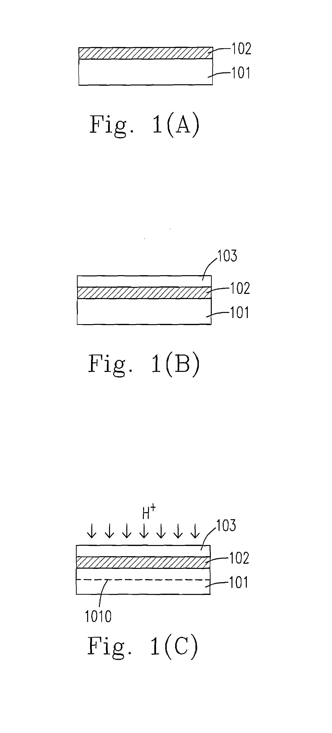
[0037]Please refer to FIG. 1(A) to FIG. 1(H), which respectively show the schematic structure and the manufacturing process of the thin film solar cell according to the present invention.

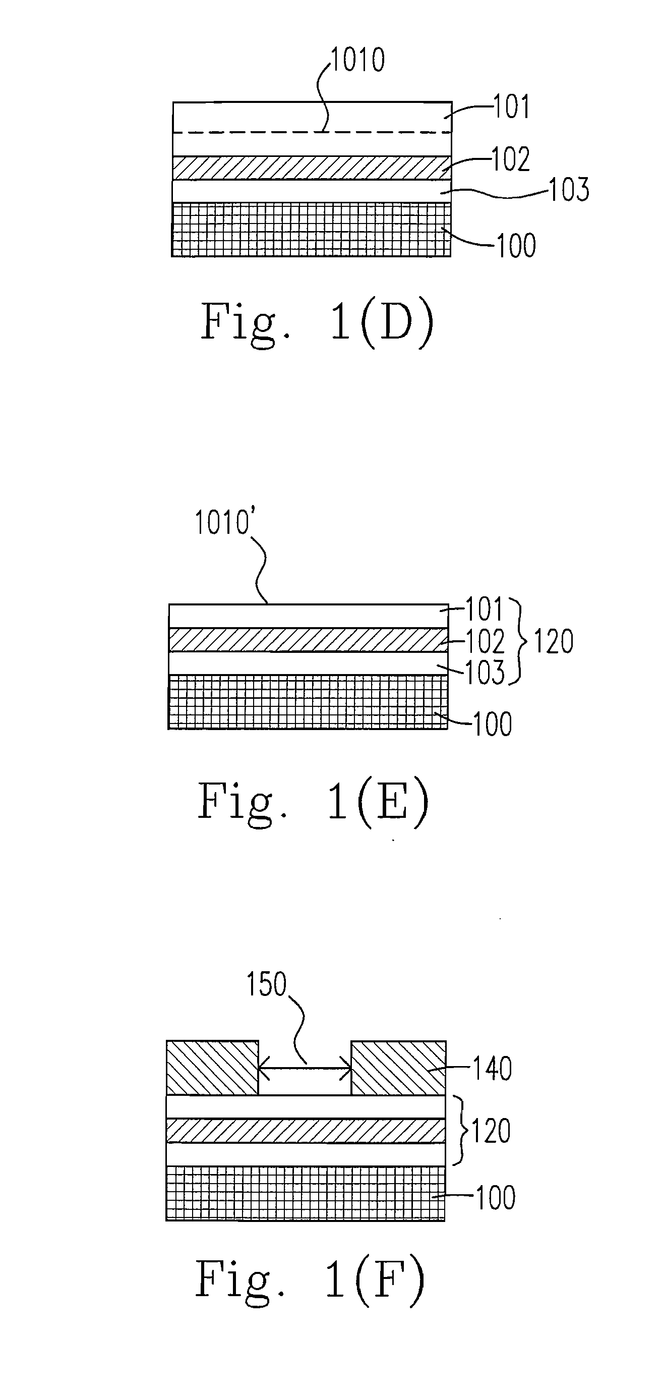
[0038]As shown in FIG. 1(A), a silicon substrate 101 having a germanium layer 102 disposed on a first surface thereof is provided. The germanium layer 102 is formed on the silicon substrate 101 through an epitaxial process preformed by one selected from a group consisting of a molecular beam epitaxy (MBE) system, a plasma enhanced chemical vapor deposition (PECVD) system, and an ultra high vacuum chemical vapor deposition (UHVCVD) system, or through a wafer bonding process. Further, as shown in FIG. 1(B), a silicon layer 103 is disposed on the germanium layer 102. Similarly, the silicon layer 103 can be formed by one of the epitaxial process and the wafer bonding process. After forming the germanium layer 102 and the silicon layer 103 on the silicon substrate 101, a hetero-junction structure made of...

second embodiment

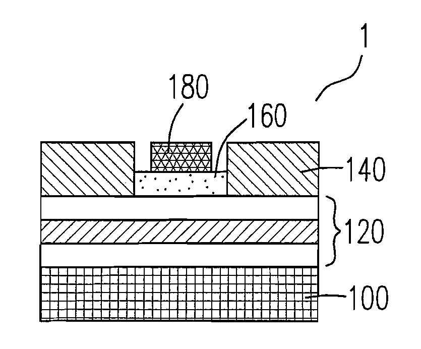
[0044]In a preferred embodiment of the present invention, the thin-film solar cell 2 shown in FIG. 2(C) could be used as one of the Metal Oxide Semiconductor (MOS) type solar cell and P-type / intrinsic / N-type (PIN) type solar cell. Moreover, the carrier substrate 100 and the first electrode layer 110 of the thin-film solar cell 2 according the present invention could be selected from a non-opaque material, so that the sunlight can enter into the thin-film solar cell from the side of the carrier substrate 100, in order to prevent the incident sunlight from being blocked by the second electrode layer 180.

[0045]Please refer to FIGS. 3(A) and 3(B), which respectively show the alternative structures of the solar cell according to the first and the second embodiments of the present invention. As shown in FIG. 3(A), the main difference between the thin film solar cell 3A and the abovementioned solar cell 1 shown in FIG. 1(H) is that the hetero-junction structure 120′ thereof is formed by mu...


PUM


Abstract

A thin-film solar cell having a hetero-junction of semiconductor and the fabrication method thereof are provided. Instead of the conventional hetero-junction of III-V semiconductor or homo-structure of IV semiconductor, the thin-film solar cell according to the present invention adopts a novel hetero-junction structure of IV semiconductor to improve the cell efficiency thereof. By adjusting the amount of layer sequences and the thickness of the hetero-junction structure, the cell efficiency of the thin-film solar cell according to the present invention is also optimized.

Description

FIELD OF THE INVENTION[0001]The present invention relates to a thin film solar cell and the fabrication method therefor, and more particularly to a thin-film solar cell having hetero-junction of semiconductor and the method for fabricating the same.BACKGROUND OF THE INVENTION[0002]Most of the solar cells according to the prior art are usually constructed by forming therein a hetero-junction structure made of the III-V semiconductor materials or a homo-junction structure made of the IV group semiconductor materials. As the solar cells hold much promise for the alternative power system, the relevant technologies for fabricating the solar cell are also well developed.[0003]For example, in the U.S. Pat. No. 5,374,564, a method for forming a homo-junction of IV group semiconductor materials by using a thin film transfer technology is provided. The method has also been well known as the “smart-cut” process. Further, in the U.S. Pat. No. 7,019,339, a method for fabricating a solar cell con...

Claims


Application Information

Patent Timeline
IPC IPC(8): H01L31/0336H01L31/18
CPCB82Y20/00H01L31/022425H01L31/022433H01L31/028H01L31/035254H01L31/035281Y02E10/547H01L31/0745H01L31/075H01L31/1804H01L31/1812Y02E10/548H01L31/072Y02P70/50
Inventor LIU, CHEE-WEEYU, CHENG-YEHCHEN, WEN-YUANLIN, CHU-HSUAN
Owner NAT TAIWAN UNIV
Why Eureka
Try Eureka