Plasma etching method and computer-readable storage medium

a technology of plasma and etching medium, which is applied in the direction of basic electric elements, semiconductor/solid-state device manufacturing, electric devices, etc., can solve the problems of lower plasma resistance of arf photoresist, and increased surface and sidewall roughness of arf photoresist, etc., to suppress surface and sidewall roughness, suppress generation of striation, and good precision

Inactive Publication Date: 2009-08-13
TOKYO ELECTRON LTD
View PDF13 Cites 20 Cited by
  • Summary
  • Abstract
  • Description
  • Claims
  • Application Information

AI Technical Summary

Benefits of technology

[0011]In accordance with the embodiment of the present invention, it is possible to provide a plasma etching method capable of suppressing roughness of a surface and sidewall of the ArF photoresist in highly anis...

Problems solved by technology

However, the ArF photoresist has a lower plasma resistance than the KrF photoresist and surface roughness occurs.
However, when a high bias voltage was ap...

Method used


Image

  • Plasma etching method and computer-readable storage medium
  • Plasma etching method and computer-readable storage medium
  • Plasma etching method and computer-readable storage medium

Examples


Embodiment Construction

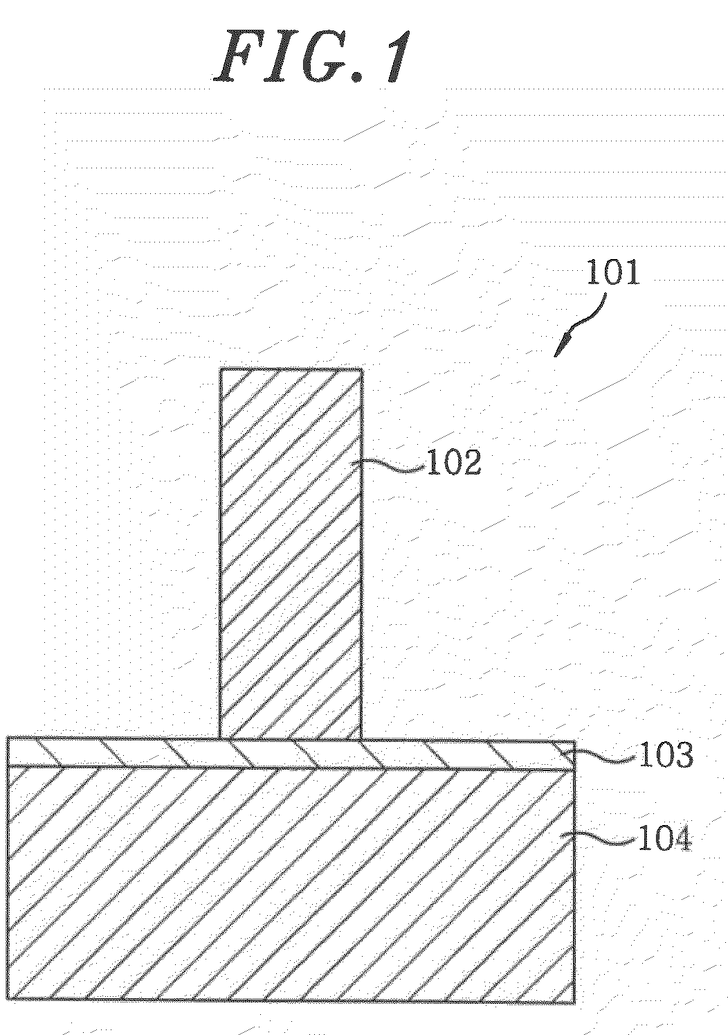
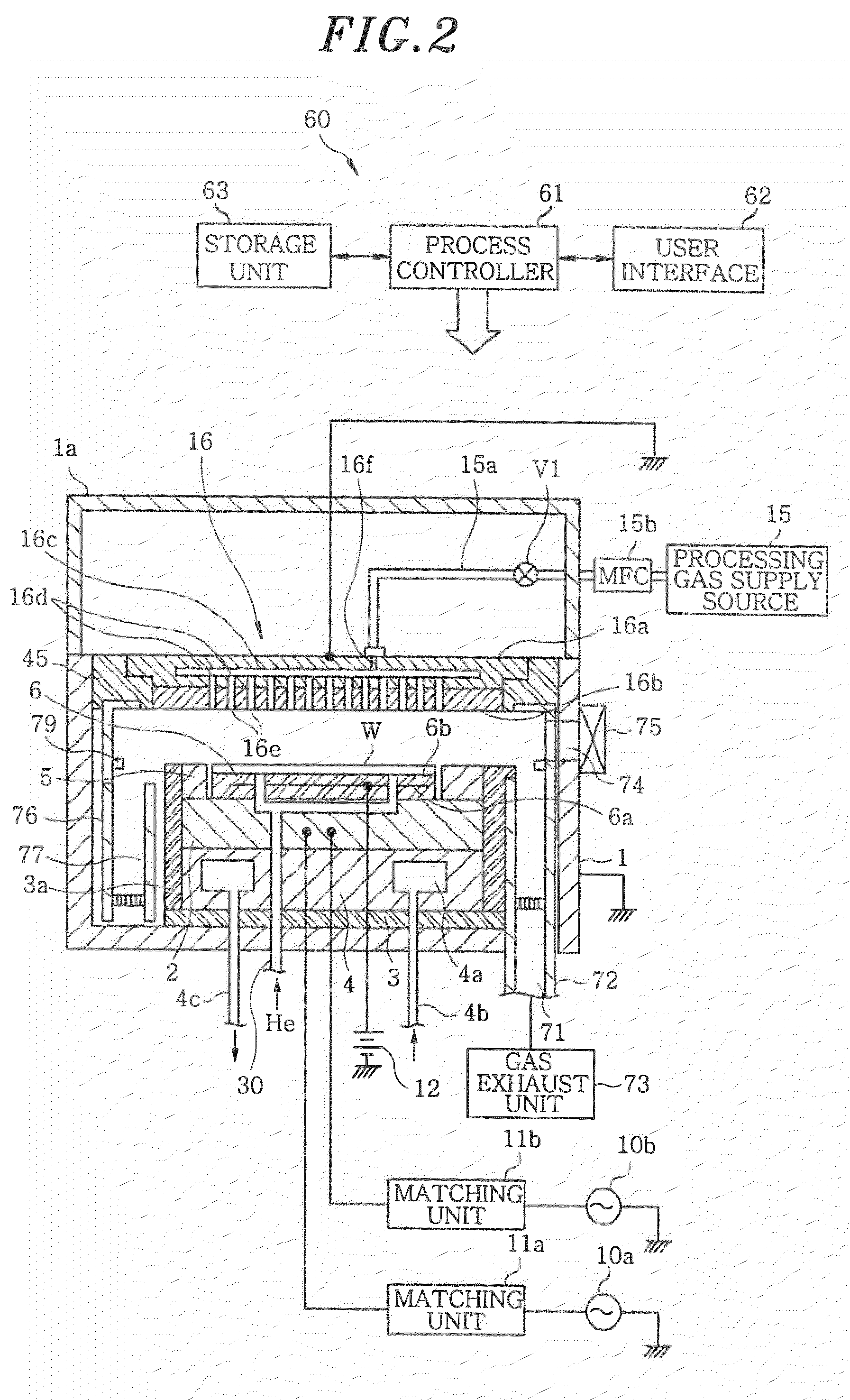
[0021]Hereinafter, embodiments of the present invention will be described in detail with reference to the accompanying drawings which form a part hereof. FIG. 1 is an enlarged view showing a cross sectional configuration of a semiconductor wafer serving as a substrate to be processed in a plasma etching method in accordance with an embodiment of the present invention. FIG. 2 illustrates a configuration of a plasma etching apparatus in accordance with the embodiment of the present invention. First, the configuration of the plasma etching apparatus will be described with reference to FIG. 2.

[0022]The plasma etching apparatus includes a processing chamber 1 which is airtightly sealed and electrically connected to a ground potential. The processing chamber 1 has a cylindrical shape and is made of, e.g., aluminum. A mounting table 2 is provided in the processing chamber 1 to horizontally support the semiconductor wafer W serving as a substrate to be processed. The mounting table 2 is mad...


PUM


Abstract

A plasma etching method includes etching an etching target layer formed on a substrate to be processed by a plasma of a processing gas by using an ArF photoresist as a mask. The etching target layer is a silicon nitride layer or silicon oxide layer, and the processing gas contains at least a CF3I gas. A high frequency power having a frequency of 13.56 MHz or less is applied to a lower electrode mounting the substrate thereon.

Description

FIELD OF THE INVENTION [0001]The present invention relates to a plasma etching method for etching an etching target layer formed on a substrate to be processed by a plasma of a processing gas by using an ArF photoresist as a mask and a computer-readable storage medium.BACKGROUND OF THE INVENTION [0002]Conventionally, in a manufacturing process of a semiconductor device, plasma etching is widely performed to etch an etching target layer such as a silicon nitride layer and a silicon oxide layer formed on a substrate to be processed by a plasma of a processing gas by using a photoresist as a mask.[0003]Further, in plasma etching, an ArF photoresist is replacing a conventional KrF photoresist to meet a demand for miniaturization of a circuit pattern in a recent semiconductor device. However, the ArF photoresist has a lower plasma resistance than the KrF photoresist and surface roughness occurs. Accordingly, for example, a technique for suppressing surface roughness of the ArF photoresis...

Claims


Application Information

Patent Timeline
IPC IPC(8): H01L21/3065
CPCH01L21/31144H01L21/31116H01L21/3065
Inventor MATSUYAMA, SHOICHIROHONDA, MASANOBU
Owner TOKYO ELECTRON LTD
Why Eureka
Try Eureka