Large -area pixel for use in an image sensor

a large-area pixel and image sensor technology, applied in the field of large-area pixel for use in an image sensor, can solve the problems of monotonous increase, high electrical power consumption, and inability to realize such conventional photo sensors that are at the same time very large and highly sensitive, and achieve the effects of low electrical power consumption, minimal electrical power consumption, and large sensing area

Active Publication Date: 2009-08-27
AMS SENSORS SINGAPORE PTE LTD
View PDF9 Cites 14 Cited by
  • Summary
  • Abstract
  • Description
  • Claims
  • Application Information

AI Technical Summary

Benefits of technology

[0013]It is an object of the invention to provide a pixel for use in a solid-state image sensor and a method for sensing incident radiation which make possible the full control over the two-dimensional lateral electric field in the semiconductor, allowing the optimized, application-specific collection and accumulation of photo-generated charge carriers with minimum electrical power consumption in a given semiconductor technology. The pixel and the method shall allow for sensing of electromagnetic radiation, preferably in the ultraviolet, visible or infrared spectral range, or particle radiation. The pixel shall simultaneously meet the following requirements: large sensing area of more than 10 square micrometers, high quantum efficiency, high photo-charge sensitivity and low power consumption.

Problems solved by technology

This capacitance, on the other hand, increases monotonously (for larger pixels almost linearly) with the pixel size.
For this reason, it is not possible to realize such conventional photo sensors that are at the same time very large and highly sensitive.
However, this implies the use of industry standard CCD technology for the fabrication of CCD image sensors, as well as suitable CCD clocking circuitry and schemes with the associated system complexity and high electrical power consumption.
The charge transport process within the semiconductor bulk material that is typical for CCD structures, is primarily based on slow diffusion processes instead of fast drift processes, hence significantly limiting the response time.
Again, system complexity and power consumption will be rather high.
Furthermore, no demodulation action for an incident modulated wave field can be obtained with such a device, since photo-charge can only be moved in one fixed direction.
Though the photo-sensitive area and the conversion capacity have been decoupled, allowing the combination of large area sensing and high sensitivity, the disadvantages of this approach include the limited demodulation speed that is obtained with CCDs, especially if large photosensitive sites and CCD gates are employed.
Further disadvantages are the necessity of special semiconductor processes for the fabrication of the CCD structures, and the demands on clocking waveforms with specially shaped rising or falling edges in order to obtain high charge-transfer efficiency under the CCD gates.
The disadvantage of the FET switch is increased charge and voltage noise behavior due to incomplete charge transfer, charge injection effects and channel current noise caused by gate voltage fluctuations.
The number of storage sites is limited to four, rendering this device ineffective if more than four samples per period of the modulated waveform should be taken.
Since the teaching also relies on switches for the transfer of photo charges from the photo sites to the storage elements, the same disadvantages are encountered as described for the above two documents.
The basic photodiode and MOS device types and the enhanced pixel structures with separate photo-charge collection area and photo-charge storage and detection devices mentioned above have the disadvantage of one-dimensional pixel topology.
As a direct consequence, in movements of photo-generated charges effectuated by drift fields, for example within the space charge region of a photodiode or between MOS devices (both with or without overlapping gate electrodes), there is very little control over the two-dimensional distribution of the electric field and, consequently, over the motion of the photo-charges.
In addition, some of the pixel structures described above exhibit high power dissipation and / or low quantum efficiency.
No known pixel device is capable of combining large-area sensing with high conversion gain, high quantum efficiency and in particular a two-dimensional spatial influence on the transport of the photo-generated charges by an optimized electric field distribution that can be fully controlled in the two lateral dimensions.

Method used


Image

  • Large -area pixel for use in an image sensor
  • Large -area pixel for use in an image sensor
  • Large -area pixel for use in an image sensor

Examples


Embodiment Construction

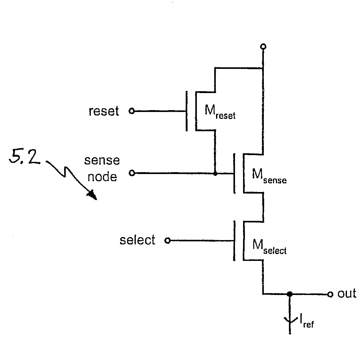
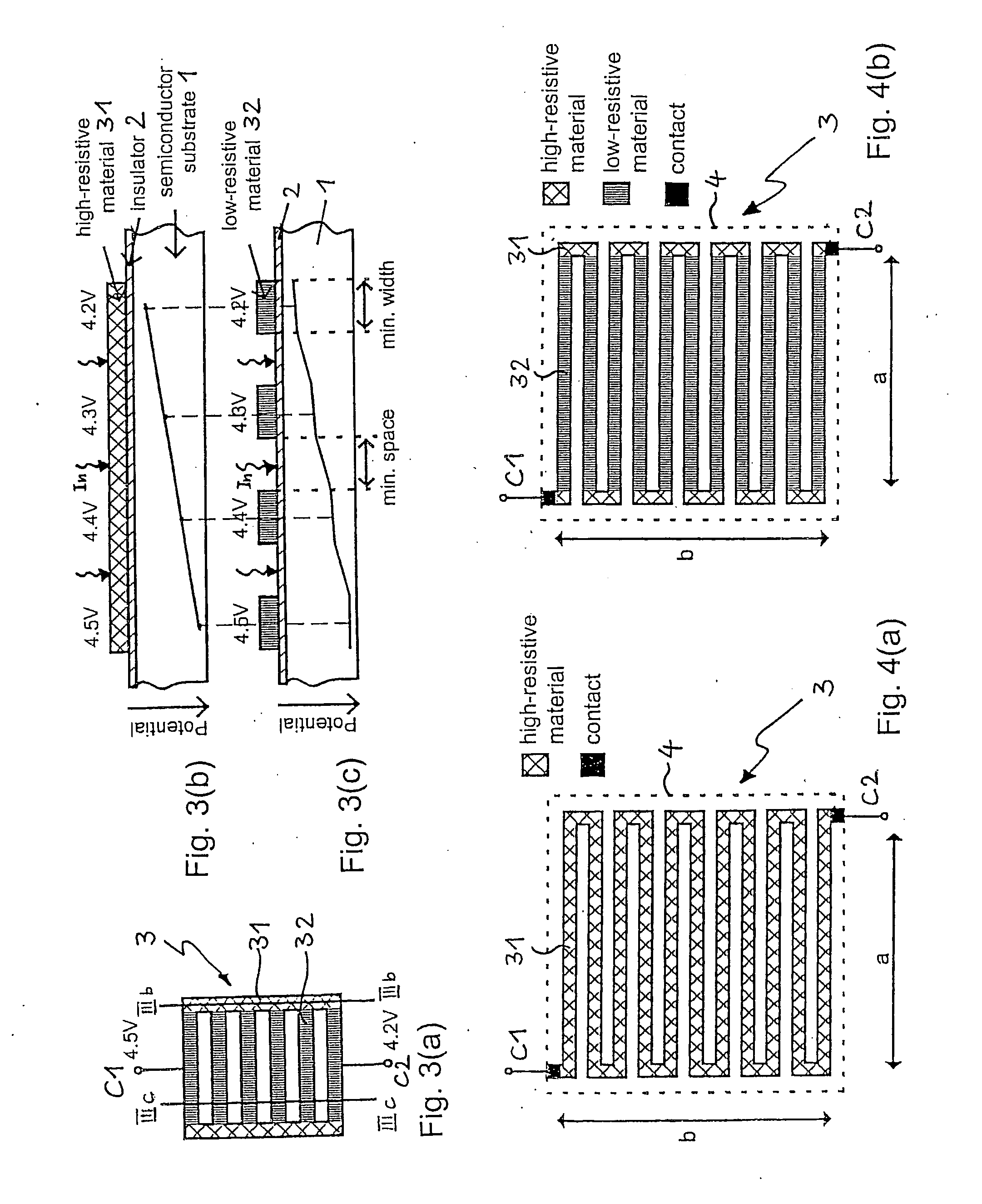
[0058]Cross-sections through an embodiment of the pixel according to the invention are shown in FIGS. 3(b) and 3(c). The new pixel architecture makes use of a semiconductor substrate 1, such as a silicon substrate, for the conversion of incident radiation In into electron-hole pairs. Without loss of generality, one can assume in the following that this semiconductor material 1 is p-doped and that one wants to detect electrons as minority charge carriers in the semiconductor material 1. All subsequent arguments can be suitably modified to hold true for the detection of photo-generated holes as minority carriers in n-doped semiconductor material. The semiconductor substrate 1 is covered with a transparent insulating layer 2, preferably an oxide, as available in industry standard CMOS processes. The oxide-layer thickness is chosen in the range of 1 nm to 500 nm, according to the specifications of the selected semiconductor process, in order to transfer a large part of the electric surf...


PUM


Abstract

A pixel for detecting incident radiation (In) over a large area with high sensitivity and low power consumption. The pixel comprises a semiconductor substrate (1), covered by a thin insulating layer (2), on top of which a dendritic or arborescent gate structure (3) is arranged. The dendritic gate (3) is electrically connected at two or more contacts (C1, C2) with voltage sources, leading to the flow of a current and a position-dependent potential distribution in the gate (3). Due to the use of arborescent structures and various materials (31, 32), the pixel can be optimized for a certain application, in particular in terms of the electric field distribution, the RC time constant, the power consumption and the spectral sensitivity. Due to its compact size, the photo sensor can be arranged in linear or two-dimensional manner for the realization of line and area sensors.

Description

FIELD OF THE INVENTION[0001]The present invention relates to all solid-state sensing and measuring techniques requiring the local detection of electromagnetic or particle radiation, preferably electromagnetic radiation in the ultraviolet, visible or infrared spectral range, while satisfying simultaneously the following constraints: large sensing area of more than 10 square micrometers, high quantum efficiency and photo-charge sensitivity, low power consumption, as well as the capability to demodulate incident modulated radiation.[0002]This invention further relates to all photo-sensing and particle-sensing applications in which it is difficult to focus the incident radiation with optical means, such as X-ray, gamma-ray, deep-UV or atom-beam imaging.[0003]This invention also relates to all optical distance measurement techniques based on optical phase-shifting interferometry or on time-of-flight ranging, requiring the local determination of the modulation parameters of incident, temp...

Claims


Application Information

Patent Timeline
Patent Type & Authority Applications(United States)
IPC IPC(8): H01L27/00
CPCH01L27/14812H01L27/14603
Inventor BUTTGEN, BERNHARDLUSTENBERGER, FELIXSEITZ, PETER
Owner AMS SENSORS SINGAPORE PTE LTD
Why Eureka
Try Eureka