Trenched mosfet with trenched source contact

Active Publication Date: 2009-08-27
FORCE MOS TECH CO LTD
View PDF1 Cites 31 Cited by
  • Summary
  • Abstract
  • Description
  • Claims
  • Application Information

AI Technical Summary

Benefits of technology

[0009]Compared with the conventional trenched MOSFET, the present invention provides good ohmic contact to sidewall of the source contact and the base resistance Rp between channel and the source contact trench is thus reduced. Otherwise, the parasitic vertical bipolar (N+-P-N bipolar, N+ is the N+-type source layer, P

Problems solved by technology

The sidewall of source contact trench has no ohmic contact (due to low doping concentration of P base) with the contact metal plug resulting in poor ruggedness performance during U

Method used


Image

  • Trenched mosfet with trenched source contact
  • Trenched mosfet with trenched source contact
  • Trenched mosfet with trenched source contact

Examples


Embodiment Construction

[0015]The present invention is described by the following specific embodiments. Those with ordinary skills in the arts can readily understand the other advantages and functions of the present invention after reading the disclosure of this specification. The present invention can also be implemented with different embodiments. Various details described in this specification can be modified based on different viewpoints and applications without departing from the scope of the present invention.

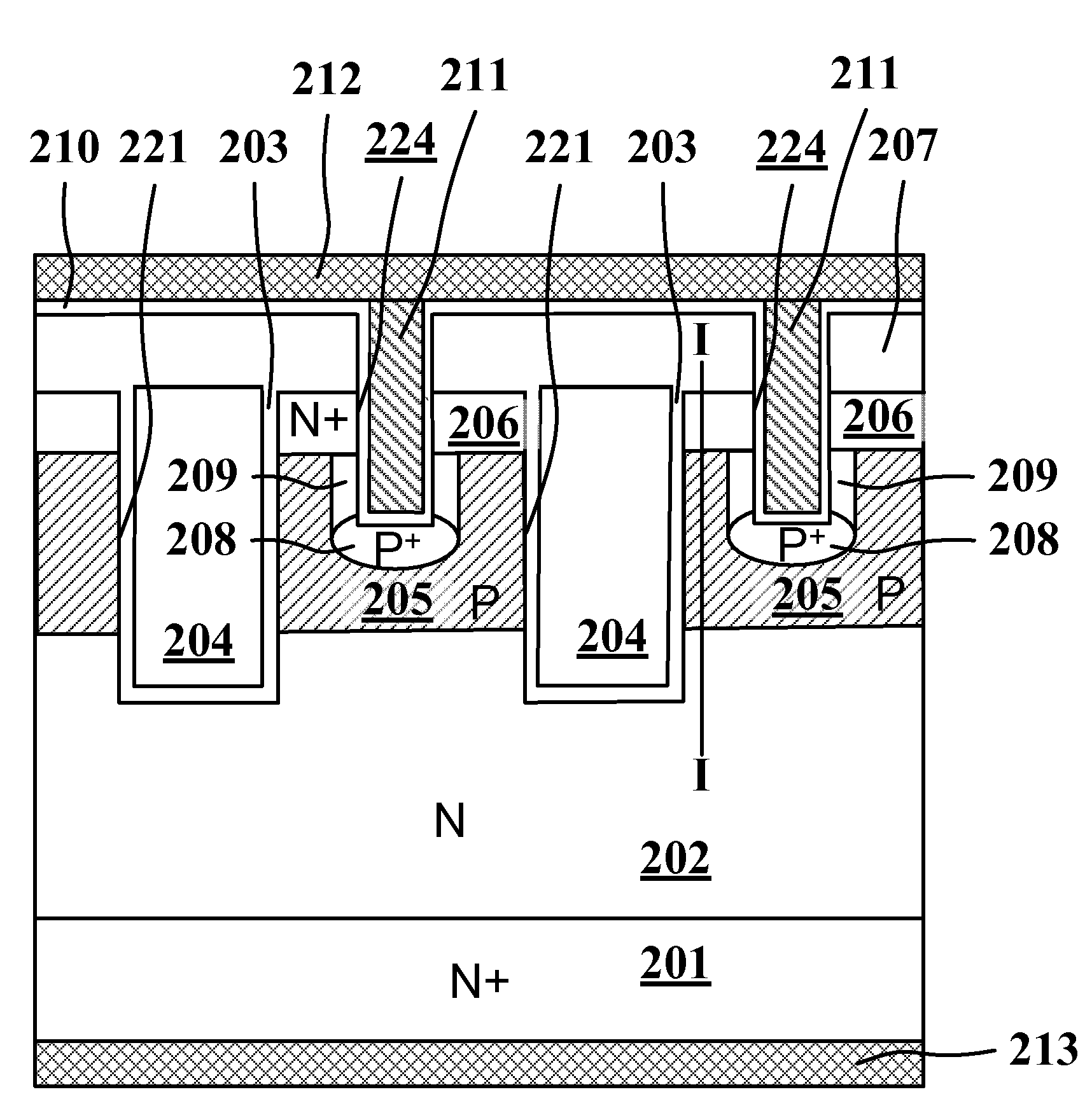
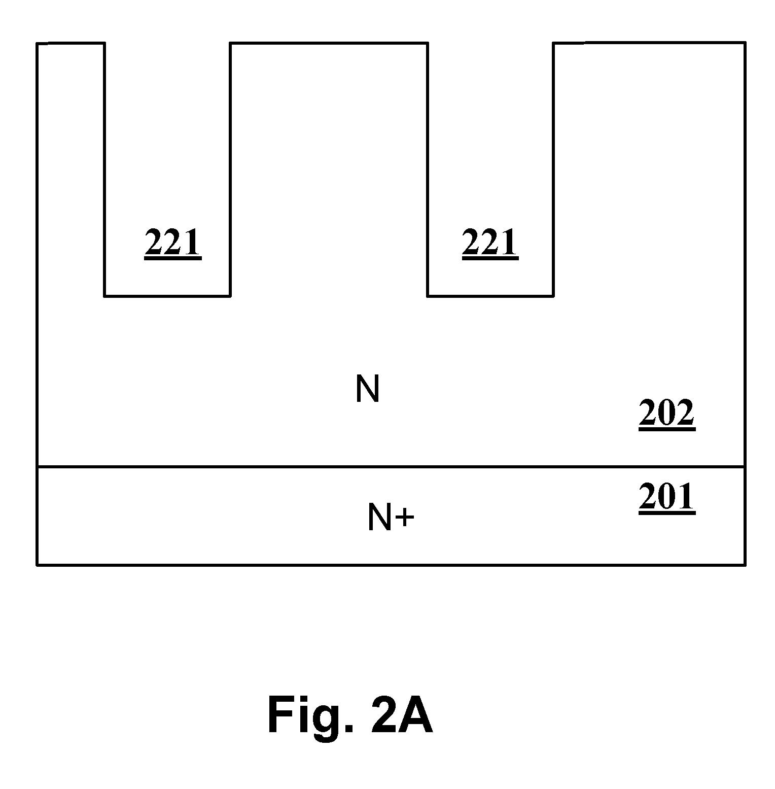
[0016]Referring to FIGS. 2A to 2F, description will be made of a method of producing a trenched MOSFET with trenched source contact according to an embodiment of the present invention.

[0017]Referring to FIG. 2A, a silicon substrate comprises a N+-type silicon substrate (201) which is strongly n-doped and haves a N-type epitaxial layer (202) which is weakly n-doped thereon. A trench mask, a sacrificial oxide (not showed in figure), is applied, and Lithography and silicon etching processes are per...


PUM


Abstract

A trenched MOSFET with trenched source contact, comprising: a semiconductor region, further comprising a silicon substrate, a epitaxial layer corresponding to the drain region of the trenched MOSFET, a base layer corresponding to the body region of the trenched MOSFET, and a source layer corresponding to the source region of the trenched MOSFET; an interlayer oxide film formed on the source layer; a front metal layer formed on a upper surface of the semiconductor region; a back metal layer formed on a lower surface of the semiconductor region; a plurality of trenched gates formed to reach the epitaxial layer through the source layer and the base layer, and is covered by the interlayer oxide film; and a plurality of source contact trenches formed to reach the base layer through the interlayer oxide film and the source layer, and is covered by the front metal layer; wherein the silicon substrate, the epitaxial layer, the base layer, and the source layer are stacked in sequence; and each of the source contact trenches has a lateral contact layer at a sidewall thereof.

Description

FIELD OF THE INVENTION[0001]This invention relates to a trenched MOSFET with trenched source contact and, in particular, to provide a lateral contact layer in the MOSFET for avalanche improvement.BACKGROUND OF THE INVENTION[0002]In the structure of a trench Metal-Oxide-Semiconductor Field Effect Transistor (MOSFET) or vertical transistor, the gate of the transistor is formed in a trench on top of an epitaxial layer—and the source / drain regions are formed on both sides of the gate. This type of vertical transistor allows high current to pass through and channel to be turned on / off at a low voltage.[0003]Referring to FIG. 1, a cross-sectional diagram of the structure of a trenched MOSFET is shown. In the prior art, the trenched MOSFET has a MOSFET structure comprises a N+-type silicon substrate (101), a N-type epitaxial layer (102), a plurality of trenches (121), an oxide film (122), a polysilicon (123), a plurality of gate oxide films (103), a plurality of trenched gates (104), a P-t...

Claims


Application Information

Patent Timeline
IPC IPC(8): H01L29/78
CPCH01L21/26586H01L29/1095H01L29/7813H01L29/66727H01L29/66734H01L29/456
Inventor HSIEH, FU-YUAN
Owner FORCE MOS TECH CO LTD
Why Eureka
Try Eureka