Semiconductor device

a technology of semiconductor devices and insulators, applied in semiconductor devices, semiconductor/solid-state device details, electrical equipment, etc., can solve the problems of affecting the efficiency of etching, affecting the peeling of interlayer insulators, and increasing the depth of trench processes for etching

Inactive Publication Date: 2009-08-27
RENESAS ELECTRONICS CORP
View PDF5 Cites 10 Cited by
  • Summary
  • Abstract
  • Description
  • Claims
  • Application Information

AI Technical Summary

Benefits of technology

[0009]An object of the present invention is to provide a technique capable of preventing the peeling of an in

Problems solved by technology

However, the technique disclosed in the Japanese Patent Application Laid-Open Publication No. 2006-318988 (Patent Document 1) includes such an issue that the depth in a

Method used


Image

  • Semiconductor device
  • Semiconductor device
  • Semiconductor device

Examples


first embodiment

[0065]Hereinafter, the first embodiment will be described in detail with reference to FIG. 4 to FIG. 14.

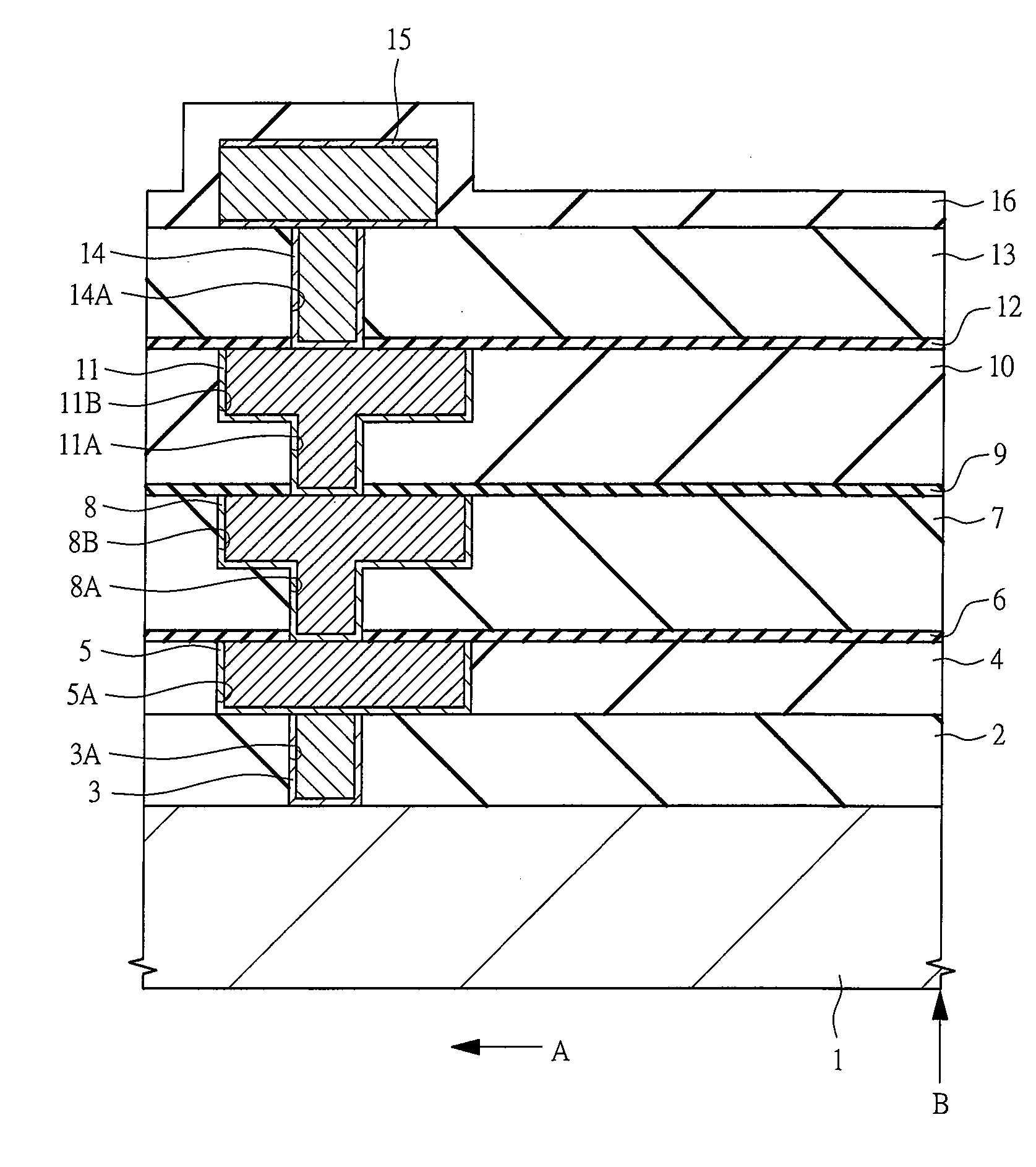
[0066]FIG. 4 is a cross section diagram of a principal part in a vicinity of an edge portion of a semiconductor device (chip) according to the first embodiment. In FIG. 4, an arrow A indicates an inward direction of the semiconductor device, and an arrow B indicates an edge portion of the semiconductor device. A circuit formation region where a semiconductor element, a wire and the like are formed is defined by the side of the arrow A.

[0067]In the semiconductor device according to the first embodiment, for example, interlayer insulators (first insulator) 2 and 4 are formed on a main surface of the semiconductor substrate 1 made of single crystal silicon or the like, and the via 3 and the buried wire (first wire) 5 are formed in these interlayer insulators 2 and 4. The interlayer insulators 2 and 4 are formed from, for example, a BPSG (Boron-doped Phospho Silicate Glass) film, a SO...

second embodiment

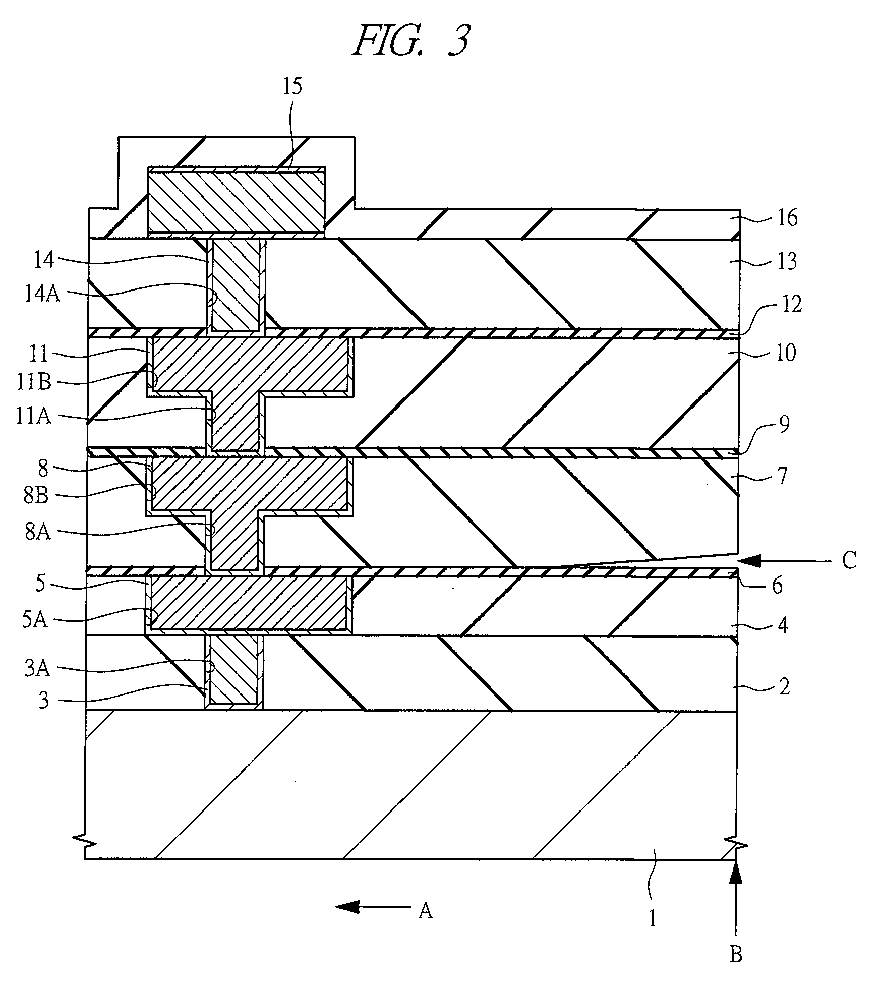
[0090]Next, a second embodiment will be described in detail with reference to the drawings. FIG. 15 is a cross section diagram of a principal part in a vicinity of an edge portion of a semiconductor device (chip) according to the second embodiment.

[0091]The difference between the first embodiment and the second embodiment lies in that not only the cap insulator 6 but also the cap insulator 9 is not provided in the edge portion of the semiconductor device.

[0092]Hereinafter, an operational effect of the semiconductor device according to the second embodiment will be described.

[0093]In the case where the interlayer insulator made of a Low-k film having relatively low Young's modulus and the cap insulator having relatively high Young's modulus are stacked in combination, the stress at the closest interface to the semiconductor substrate 1 is largest. However, depending on a form, a structure, and a material to package the semiconductor device or a use environment of the package, the str...

third embodiment

[0095]Next, the third embodiment will be described in detail with reference to FIG. 16. FIG. 16 is a planar layout diagram for describing the non-providing portion 31 of the cap insulator 6 (cf. FIG. 4 as well) in a semiconductor device according to the third embodiment.

[0096]The difference between the third embodiment and the first embodiment lies in that the non-providing portion 31 of the cap insulator 6 is formed only in the vicinity of the chip corners of the semiconductor device 21. The non-providing portion 31 according to the third embodiment has a width of at least about 1 μm or more from the chip corner toward the in-plane center direction, and more preferably has a width of about 5 μm or more.

[0097]Hereinafter, an operational effect of the semiconductor device according to the third embodiment will be described.

[0098]As described in the first embodiment, the stress generated in the thermal cycle test in the assembly process after sealing the semiconductor device 21 with r...


PUM


Abstract

In a semiconductor device having a Low-k film as an interlayer insulator, peeling of the interlayer insulator in a thermal cycle test is prevented, thereby providing a highly reliable semiconductor device. In a semiconductor device having a structure in which interlayer insulators in which buried wires each having a main electric conductive layer made of copper are formed and cap insulators of the buried wires are stacked, the cap insulator having a relatively high Young's modulus and contacting by its upper surface with the interlayer insulator made of a Low-k film having a relatively low Young's modulus is formed so as not to be provided in an edge portion of the semiconductor device.

Description

CROSS-REFERENCE TO RELATED APPLICATION[0001]The present application claims priority from Japanese Patent Application No. JP 2008-045666 filed on Feb. 27, 2008, the content of which is hereby incorporated by reference into this application.TECHNICAL FIELD OF THE INVENTION[0002]The present invention relates to a semiconductor device. More particularly, the present invention relates to a technique effectively applied to a resin-sealed semiconductor device using a low dielectric constant film (Low-k film) as an insulator between wiring layers.BACKGROUND OF THE INVENTION[0003]In recent years, with the scaling down of a transistor for achieving higher integration and higher speed in LSI, a problem of signal delay of a wire has become more and more obvious. For its solution, reductions of a wire resistance and a capacitance between wires have been desired. Accordingly, for the purpose of reducing the capacitance between wires, a wiring layer formation technique using a low dielectric const...

Claims


Application Information

Patent Timeline
IPC IPC(8): H01L23/532
CPCH01L23/3128H01L23/53238H01L2924/01015H01L2924/12041H01L2224/45147H01L2224/48247H01L2224/32225H01L2224/16225H01L2924/15311H01L2224/73204H01L2224/48227H01L2224/16227H01L24/48H01L23/585H01L23/53295H01L2924/00H01L24/45H01L2224/45124H01L2224/48091H01L2924/00014H01L2924/181H01L2924/00015H01L2924/00012H01L2224/0401
Inventor KUMAGAI, YUKIHIROOHTA, HIROYUKITANAKA, NAOTAKAFUJISAWA, MASAHIKOOHSAKI, AKIHIKO
Owner RENESAS ELECTRONICS CORP
Why Eureka
Try Eureka